13
$\begingroup$

Consider this reverse biased diode :
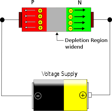
enter image description here

I read that no or very small current flows in reverse biased diode as depletion layers get widened and huge resistance is offered so no electrons can cross it. But, why the electrons or holes need to cross the depletion layer? In the diagram above, the positive charges (holes) are moving towards left and the current due to electrons is also in left, so won't the circuit be completed?

$\endgroup$
2
  • $\begingroup$ The question went unnoticed by experts for some reason. See physics.stackexchange.com/q/111899 for quality answers. $\endgroup$ Commented Oct 24, 2014 at 9:06
  • 1
    $\begingroup$ By the way the red–grey–green picture is a dangerous (partially true but actually deceiving) thing. Namely, it misleads about the charge density. $\endgroup$ Commented Oct 25, 2014 at 8:18

2 Answers 2

16
$\begingroup$

The current flows shown in the diagram are only temporary and flow only when the battery is first connected.

When you first connect the battery holes flow to the left (in your diagram) and electrons flow to the right, and the resulting charge separation creates a potential difference across the depletion layer. The flow stops when the potential difference across the depletion layer becomes equal and opposite to the battery potential. At this point the net potential difference is zero so the charges stop flowing.

$\endgroup$
9
  • $\begingroup$ How can the potential difference across the depletion layer be opposite to the battery potential? The potential in the depletion layer is from N to P and due to battery is from positive to negative terminal, so they both are in same direction, right? $\endgroup$ Commented Jan 23, 2014 at 10:53
  • 1
    $\begingroup$ Because when you pull holes away to the left you leave behind a net negative charge, and likewise when you pull electrons to the right you leave behind a net positive change. $\endgroup$ Commented Jan 23, 2014 at 11:09
  • 2
    $\begingroup$ No, you get a negative charge to the left of the PN boundary and a positive charge to the right. $\endgroup$ Commented Jan 23, 2014 at 11:39
  • 1
    $\begingroup$ Ayush, think of the gray section (depletion region) as a capacitor, the right side is left with a positive charge (electrons removed) and the left side is left with a negative charge (holes removed), so it acts like an internal battery with its positive end connected to the positive end of the external battery and likewise the negative side, therefore the "internal battery" is opposing the external battery! $\endgroup$
    – Guill
    Commented Mar 27, 2014 at 8:16
  • 1
    $\begingroup$ @JohnRennie Also do we have to neglect reverse saturation current here? $\endgroup$
    – user184271
    Commented Mar 2, 2018 at 9:40
0
$\begingroup$

This is because in case of reverse bias, p side has lots of -ve ions & n side has +ve ions vice verss. This increase in the number of ions prevents current flow across the junction by majority carriers. eg. electrons can't complete the loop as they experience resistance of -ve ions on the p side.

Check this likn : http://electriciantraining.tpub.com/14179/css/Reverse-Bias-33.htm

$\endgroup$
1
  • $\begingroup$ Are you claiming that ionization occurs in the doped semiconductor? I don't think that's correct. $\endgroup$
    – PM 2Ring
    Commented Aug 21, 2018 at 5:36

Your Answer

By clicking “Post Your Answer”, you agree to our terms of service and acknowledge you have read our privacy policy.

Not the answer you're looking for? Browse other questions tagged or ask your own question.