I am not able to understand why the PN junction does not conduct when reverse biased. Can't electrons travel from the N side through the power supply to the P side where they can jump from one hole to other to traverse the P side and then cross the depletion layer back in to the N region ?
-
$\begingroup$ A DC power supply only permits charges to flow one way. $\endgroup$– rob ♦Commented May 9, 2014 at 4:27
-
$\begingroup$ Where am I indicating that current is going in the reverse direction ? $\endgroup$– user46169Commented May 9, 2014 at 5:14
-
$\begingroup$ If the N side is connected to the positive terminal of a battery, the electric field will attract electrons from the N side to the positive terminal ? Electrons will leave the battery's -ve terminal and go to the P side and then through the holes to the N side. Where are the electrons moving against the electric field ? $\endgroup$– user46169Commented May 9, 2014 at 6:19
-
$\begingroup$ An earlier question about the same thing: physics.stackexchange.com/questions/94915/… How can they be merged now? $\endgroup$– Incnis MrsiCommented Oct 24, 2014 at 9:00
-
$\begingroup$ Well I think we should keep this one, but I'm ... biased. $\endgroup$– rob ♦Commented Oct 27, 2014 at 16:59
3 Answers
Think about why the diode does conduct current when it is forward-biased.
In that case, there is an electric field pointing from the P-type end to the N-type end. Negative electrons want to climb up the field. The electrons get to the junction and find holes to fall into. Now that the electrons are in the P-type material they can find their way to the electrode and get pushed through the power supply to complete the circuit.
When the diode is reverse-biased, the electric field points from the N-type to the P-type end. The negatively charged electrons want to climb up the field, so they move away from the junction up towards the N-type electrode. The positively charged holes in the P-type material want to fall down the field, so they move away from the junction down towards the P-type electrode. Now there is a "depletion region" around the junction where there are very few charge carriers of either sign.
Without any charge carriers, the depletion region acts sort of like an insulator, and the junction acts sort of like a capacitor with an insulator in its gap: once a certain amount of charge has flowed to the sides of the gap, the capacitor is "full" and the current stops. The difference between a capacitor gap and a charge-depleted junction is that if the voltage applied from the battery is removed, the charges on either side of the depletion region will be free to move towards each other and the diode will not permanently store any charge.
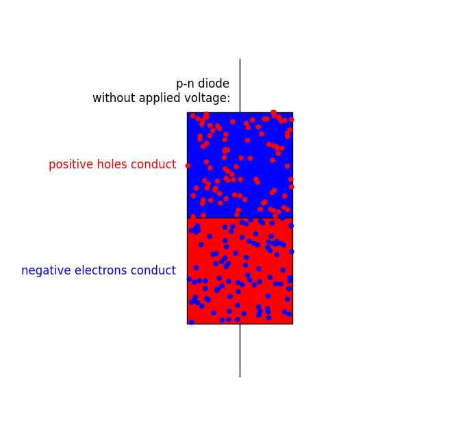
Since we're still going back and forth on this I've drawn you some pictures. Here's a silly cartoon showing the distribution of charges in the diode without any applied voltage:

The mobile charge carriers and their substrates are colored according to their charges: the p-type material has conducting positive holes that can move on a negative substrate, while the n-type material has conducting mobile electrons that can move on a positive substrate. (If you're really stuck on this question, I think it might be here: even though we "know" that the p-type semiconductor is made of protons, neutrons, and electrons, the charge carriers are quasiparticles with positive charge and effective mass comparable to the electron mass.)
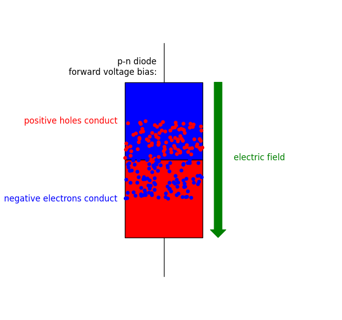
Now let's forward-bias the diode:

The "forward" electric field drives both sorts of charge carriers towards the junction, where they interact with each other. The electrons are able to fall into the holes — or the electrons and the holes are able to annihilate, if you like that better — which causes charge to move across the junction. Moving charges mean you have conduction.
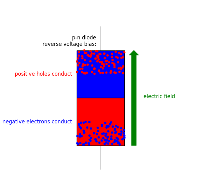
Finally let's reverse-bias the diode:

Now the electric field applied by the power supply to the diode pulls both sorts of mobile charges away from the junction. You can't have current flow across the junction because none of the charges near the junction are mobile: the mobile charges have all left, and the remaining charges are fixed to the crystal lattice, as in an insulator.
You ask what would happen to an electron that entered the p-type material from the terminal at the top of my drawing, if the diode is reverse-biased. That electron would fill one of the holes clustering around that terminal. With one hole fewer, the remaining holes are free to cluster a little closer to the terminal. This will polarize the material until the internal electric field vanishes (I suppose my green arrows should have been labeled "applied electric field"), at which point the charge flow stops.
-
$\begingroup$ Why can't an election (which has entered the P region from the -ve terminal and jumped from hole to hole to reach the depletion region) cross the depletion region into the N side aided by the electric field. Can't one electron enter the depletion region if at the same time another electron leaves the P side's depletion region and enters the N side. Can't the ions in the P side's depletion region allow electron flow. $\endgroup$ Commented May 10, 2014 at 3:10
-
$\begingroup$ In the P region the holes carry the current, not the electrons. The reverse-bias field pulls the holes away from the junction until the voltage drop across the junction matches the voltage drop across the power supply. After all the charge carriers have left, the depletion layer near the junction is insulating. $\endgroup$– rob ♦Commented May 10, 2014 at 7:17
-
$\begingroup$ Thanks for your patience. If we apply a voltage to a bar made of a p-type semiconductor, we have hole flow inside the bar and electron flow in the wire connecting to a battery. Electrons enter the P type bar (from the -ve terminal) from one side and exit the P type bar on the other side to reach the +ve terminal. Why can't this happen in the P region of a diode ? $\endgroup$ Commented May 11, 2014 at 2:42
-
$\begingroup$ In your second example, the electrons enter the P-type material from the conducting negative terminal. But in a diode, the N-type material on the other side of the junction is also depleted of charge carriers. $\endgroup$– rob ♦Commented May 11, 2014 at 2:45
-
1$\begingroup$ Rob, thanks for the nice explanation. I think I get it now. $\endgroup$ Commented May 13, 2014 at 5:27
A reverse-biased PN junction does in fact conduct current, just not very much.
A reverse-bias voltage depletes the minority-carrier charge concentrations below their equilibrium values, say by a total amount of charge $Q$. Since recombination (with time constant $\tau$) tends to restore equilibrium, a reverse current $Q/\tau$ is required to sustain the depletion.
This reverse current is small because there aren't many minority carriers to deplete. (Conversely, for a forward bias, excess minority-carrier concentrations, and consequently currents, can be large.)
Note that at higher temperatures, the equilibrium minority carrier densities increase, and so does the reverse current.
Update: Re the question of "extra" electrons injected into the P material increasing the reverse current: if such an electron could reach the junction, it would indeed be swept into the N material by the junction field. However, these extra electron can't make it to the junction: their presence would make the P material electrically negative instead of neutral, and so would create a blocking electric field.
There's an interesting and very important device that illustrates this blockage by side-stepping it: a bipolar junction transistor.
An NPN transistor under standard bias conditions features a reverse-biased PN junction (connected between a collector N region and base P region), just like the device under consideration here, plus a second PN junction between the base P region and an emitter N region. The P region is physically thin.
If the second PN junction (between base and emitter) is forward-biased, electrons can now be injected into the base P region from the emitter, because charge neutrality in the P region is maintained by current from the base contact. (This neutrality-maintaining mechanism is what's missing in the plain reverse-biased PN junction.)
Because the P region is thin, these injected electrons are more likely to reach the base/collector junction, and be swept across it, than to recombine in the base. This mechanism is transistor action, as explained here.
Update: This expression for reverse-bias current is an example of stored-charge analysis (see, for example, Gibbons, Semiconductor Electronics, section 6.4.7, or here. Here is a sketch of that analysis.
Stored-charge analysis focuses on the minority charge carrier densities near the junction. For specificity, consider the holes in the n-type material. When the diode is forward-biased, there is an excess of these holes compared to their number when the applied voltage is 0, amounting to an excess charge $Q_p$. This excess charge will recombine in the hole lifetime $\tau_p$. In steady-state, therefore, this charge must be replaced by new holes from the p-region, resulting in a hole current $Q_p/\tau_p$. Similarly, there will be an electron current $Q_n/\tau_n$, and the total current $i$ will be the sum of these two:
$$ i = \frac{Q_p}{\tau_p} + \frac{Q_n}{\tau_n} $$
$Q_p$ is evaluated by integrating the excess-hole-density $ p_E(x)$, with $x=0$ at the junction:
$$ p_E(x) = p_E(0) e^{-x/L_p} \,\, , \, p_E(0) = p_n \left( e^{qv/(kT)} -1 \right) $$
where $L_p$ is the hole diffusion length in the n-material, $p_n$ is the minority hole density in the n-material far from the junction, $v$ is the applied voltage, $q$ the carrier charge, $k$ Boltzmann's constant, and $T$ the temperature.
$$ Q_p = qA \int {dx \, p_E(x)} = qA L_p p_E(0) = qA L_p p_n \left( e^{qv/(kT)} -1 \right) $$
where $A$ is the junction area. Similarly:
$$ Q_n = qA L_n n_p \left( e^{qv/(kT)} -1 \right) $$
Combining, we get the standard diode I-V relationship: $$ i = I_0 \left( e^{qv/(kT)} -1 \right) \, \, , \, I_0 = qA \left( \frac{L_p p_n}{\tau_p} + \frac{L_n n_p}{\tau_n} \right) $$
$I_0$ is generally a very small current, by design. For forward voltage bias ($v>0$), the current gets large because of the exponential function. Conversely, for a reverse-biased junction, the exponential term asymptotes at 0 and the current $i_{v<<0} = - I_0$.
-
$\begingroup$ Electrons are the majority carriers on the N side. Why don't these electrons move to the positive terminal of the battery ? For each electron entering the +ve terminal, one electron will leave the -ve terminal towards the P side of the diode. I am sure I am missing something big but what ? $\endgroup$ Commented May 9, 2014 at 6:47
-
1$\begingroup$ @user46169 because after some time they cease to have high concentration: there's no source of refilling the N side with electrons, so the N side becomes depleted of its major carriers. After some electrons have gone to positive terminal, the high current will stop. The remaining ones are kept there by net positive charge remaining after the escaped electrons. Only the reverse current through the PN junction will refill the N side with electrons. $\endgroup$– RuslanCommented May 9, 2014 at 9:56
-
$\begingroup$ “A reverse-bias voltage depletes the minority-carrier charge concentrations” is blatantly wrong. What characterize the depletion region is low concentration of majority carriers. $\endgroup$ Commented Oct 22, 2014 at 8:59
-
$\begingroup$ @IncnisMrsi, yes, the depletion region is formed by depleted majority carriers. However, if you want to understand how much current flows in a reverse-biased diode (the question I'm addressing) you must focus on the minority carriers (the ones the applied field can sweep across the junction), and minority carrier concentrations are in fact depleted by a reverse bias. It's not an exclusive-or situation. $\endgroup$ Commented Oct 22, 2014 at 17:49
-
1$\begingroup$ @IncnisMrsi, 1) Thanks, my wording was poor; I've attempted to improve it. (I meant excess in comparison with the unbiased junction.) 2) I concur. Apparently this ideal diode characteristic works fairly well in germanium diodes (because $I_0$ is larger than for silicon?), but in Si, other mechanisms, like carrier generation in the transition region, cause the reverse-bias current to vary with voltage. $\endgroup$ Commented Oct 23, 2014 at 18:48
As far as Ī read it, rob’s answer (see above) is basically correct. But Ī’d point on two things: downplayed implications for electrostatic field, and a misconception that the depletion region forms an insulator (rob worded it as “acts sort of like an insulator” that is careful enough, but declined to comment explicitly on the nature of that substance).
Due to electronic structure of N-type semiconductor (see details at Effect of doping on the width of depletion layer of PN-junction diode ), a depleted N-type semiconductor has a strong positive volume charge. Likewise, a depleted P-type semiconductor has a strong negative volume charge. Together two sides form a double layer, that actually “holds” the voltage drop in a shallow neighborhood of the junction. There is no abrupt change of ponential and infinite field strength as infinitely-thin layer (simplistic) theory predicts, but there is a strong field.
From the point of view of band structure, the depletion region consists of a semiconducting substance. There is the same gap between conduction and valence zones as in a regular semiconductor. The thing that makes it to “act like an insulator” is a strong electrostatic field effected by a double charged level. That field brushes carriers of either sign from the region, but due to its semiconductor nature they are persistently created, accounting for a small current that flows through a reverse-biased diode.
