I know that the question "why can't a reverse biased diode conduct" has been asked before (here and here), but I'm asking it from a bit different perspective.
Why can't we inject electrons into the conduction band of the p-type material, which then would fall down the junction into the conduction band of the n-type material, and vice versa, inject holes into the valence band of the n-type material, which would climb up the junction to reach the valence band of the p-type material? This would even be energetically favourable, since this way both carriers would move through the reverse biased built-in potential which is their natural movement direction, not like in the case of forward bias, where they have to move by diffusion.
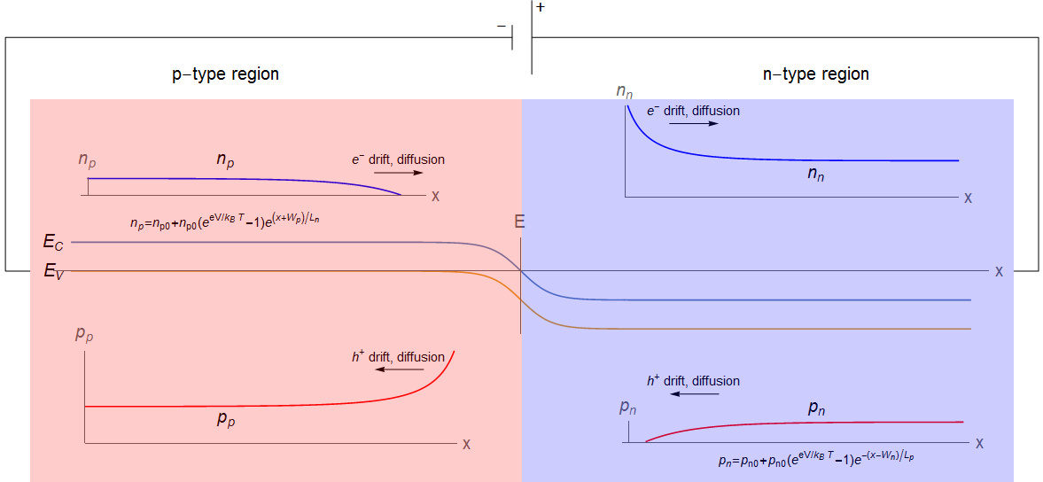
I have been thinking a lot about this, but still couldn't understand, so I'm updating the question. I meant injecting charge from the electrodes (suppose that they are ideal, non-rectifying), not injecting (e.g. photo-) generated charge through the depletion region. I have drawn a figure, which shows the charge carrier concentrations and energy levels in the diode in case of a reverse bias. To be honest, in case of the majority carrier concentrations in a region, I just simply took the $n_i^2/\text{minority carrier concentration}$, which is not exactly true near to the junction, due to the Fermi levels being separated (so this might be the trick). The "$0$" index denotes equilibrium concentrations, when there is no junction formed, there is just the p- and the n-type material, separate from each other. The way I see it, both the concentrations, and the electric field is such, that there could be current flowing. So my question remains, why can't be electrons injected from the (ideal!) contacts to the conduction band of the p-type material, and holes into the valence band of the n-type material, which would permit a (quite huge) reverse current.

