7
$\begingroup$

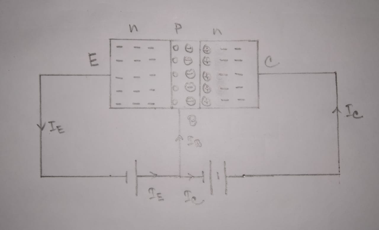
Transistor picture

Here we can see a Bipolar Junction Transistor (BJT), which has a common base configuration. My instructor recently explained to me its working principle, but I didn't understand his explanation completely as I had some issues with his explanation. His explanation was as follows:

The emitter is very heavily doped, and the base is very, very thin and very lightly doped. The collector is moderately doped.

We have two voltage sources, one having a significantly greater voltage than the other. The DC source with the higher voltage, A, is connected in reverse bias to the base-collector diode, and the DC source with the lower voltage, B, is connected in forward bias with the emitter-base diode. Upon being connected in reverse-bias, the depletion zone of the base-collector diode widens.

Now, as the emitter-base diode is connected in forward-bias with B, electrons will start to flow from the negative terminal of B with an aim to move to the positive terminal of B. However, upon reaching the base, electrons find very less holes compared to their number. So, a very small number of electrons recombine with the holes in the base and generate a small current $I_B$ flowing towards the base ($i$). The rest of the electrons, which are most of them (about 95%), being attracted by the positive donor ions of the other side of the depletion zone of base-collector diode, scoot over to the collector and move towards the positive terminal of A ($ii$). Thus, a much greater current than $I_B$, $I_C$ flows from the positive terminal of A to the negative terminal of A.

My issues:

  1. My first issue is with ($i$): current doesn't move by means of recombination of electrons and holes! Current moves by means of flow of free electrons or holes. Why did my instructor mention this? I'm very confused.
  2. My second issue is with ($ii$): electrons feel attracted to the positive donor ions on the other side of the depletion zone. According to my instructor, that's why the electrons scoot over to the collector and move towards the positive terminal of A, but my question is, the electrons should feel equally repelled by the uncovered negative acceptor ions in the base. So, why do the electrons move to the positive terminal of A?
$\endgroup$
1

3 Answers 3

6
$\begingroup$

Issue#1. There are various aspects to consider here, let me skip for a moment.

Issue#2. Ok, I think I see what your instructor means but it might be indeed a bit confusing.

  • First of all: outside the depleted region at the EB and BC junctions, in the non-depleted portion of the base (I don't see it in you sketch but it is there, at least in normal conditions), the electric field is in general very very small... for what concerns minority carriers you can assume $\vec{E}\approx\vec{0}$ in the non-depleted base (you can call this QNR, "quasi neutral region"). The reason why this happens is not completely trivial, but it has to do with screening by majority carriers.

  • Minority carriers (electrons, in your NPN) injected into the base by the directly biased EB junction are not attracted by anything, the current is vastly dominated by random diffusion rather than drift due to any residual electric field that might be present. Electrons just go around and explore the base, randomly. In general, diffusion just drives particles from regions of high density (the E-edge of the base) to regions of low density (the C-edge of the base).

  • When one electron, after diffusing randomly in the base, reaches the depletion region of the BC junction then, YES, it is swept away into the collector by the electric field of the BC junction, which is basically caused by the attraction by the donors in the C, as you mentioned.

So, you see in the end this has something to do with the "attraction by the donors in the C" but it is not so simple. Let's say donors in C create the density gradient in the base by removing any electron reaching the BC boundary. This in turn, somewhat indirectly, is what drives the diffusion of electrons through the base...

Clearly "attraction by donors in the E" does not have any similar effect, so hopefully, this solves your paradox: the EB junction is directly biased and it is doing quite the opposite of the BC one, it boosts minority carrier concentration, again driving diffusion... away from E.

Rewind to issue#1. The electrons in the base (minority carriers) that reach the BC junction are sucked into the collector and are by far the main contribution to the $I_C$ current. In principle, you also have holes injected from C to B... but this should be super-negligible in the active configuration. A direct calculation of $I_B$ is not obvious, better to calculate $I_E$ and then do $I_B=I_E-I_C$. Well... $I_E$, i.e. current crossing the EB boundary, is due to

  • Electrons injected from E to B, i.e. those we discussed above.
  • Holes injected from B to E.

In your description, you are somehow neglecting the second term (but it's there!) so let me just neglect it as well otherwise we need to open a further point. You see that $I_E-I_C$ is just due to the electrons injected in the base (thus contributing to $I_E$) that are somehow not able to reach the C end (thus contributing to $I_C$). So you see that it is quite correct to calculate $I_B$ as corresponding to charge lost per unit time by recombination in the base.

[Edit] Possibly useful further comment. If you want to get the whole picture, I really advise you to look into that B$\rightarrow$E hole current that we neglected above, because that is not irrelevant. Actually, transistors typically have a base that is short with respect to the diffusion length, implying that recombination in the base might be not so important (in the "short base approx" you even neglect it completely). In that limit, $I_B$ is actually mostly linked to that hole current in the EB junction, rather than to recombination in B. Then you'll see that all the typical design rules of thumb make pretty much sense: you want large E doping (minimizes that hole current share in the EB junction), you want a low B doping (maximizes the electron injection in B, improves diffusion which in turn boosts $\beta$ and lowers response times)... you don't want a too low B doping otherwise you might fully deplete B when reverse biasing BC, and that is bad (you get a "punch through" and everything falls apart, probabily including the device itself).

$\endgroup$
1
$\begingroup$

The emitter is very heavily doped, and the base is very, very thin and very lightly doped. The collector is moderately doped.

Typically the emitter is the most heavily doped, the collector is the most lightly doped, and the base is somewhere in the middle.

current doesn't move by means of recombination of electrons and holes! Current moves by means of flow of free electrons or holes. Why did my instructor mention this? I'm very confused.

One of the types of current often discussed in semiconductors is "recombination current". It is the current that flows to make up for carriers that recombined. As the carriers injected from the emitter into the base recombine, additional carriers are injected from the base to make up for these.

electrons feel attracted to the positive donor ions on the other side of the depletion zone. According to my instructor, that's why the electrons scoot over to the collector and move towards the positive terminal of A, but my question is, the electrons should feel equally repelled by the uncovered negative acceptor ions in the base. So, why do the electrons move to the positive terminal of A?

I don't think your instructor's explanation as worded here is correct. Lets assume an npn for this example. Swap electrons and holes in my explanation to get the same idea for pnp.

First, lets talk about the reverse biased base-collector junction. There aren't a whole lot of electrons in the base because it is p-type. But those that are there move around randomly. Some will find themselves at the edge of the depletion region and will fall down that energy slope contributing to the diode reverse saturation current.

Now, lets introduce the emitter. The forward biased emitter-base junction injects a whole bunch of extra electrons into the base. These naturally diffuse across the base and reach the base-collector junction where they all fall down the energy slope.

Adjusting the base-emitter voltage allows you to adjust the amount of electrons that are injected into the base and therefore modulate the current through the device.

$\endgroup$
1
$\begingroup$

First, note that your circuit diagram shows the flow of conventional current which can be very confusing to a student trying to understand the operation of a diode, never mind a transistor. Reversing the arrows of your diagram to show electron flow shows more clearly the physics of what's going on:

Electrons flow from the connected negative battery terminal into the emitter in a high energy state as n-carriers, then move into the base where they can diffuse into the collector region remaining in their high energy state as n-carriers, or move into a vacant lower energy state in the base aka combine with a 'hole', and emitting a photon. If it diffuses into the collector region, then this will disrupt the electrical equilibrium of the collector so that an electron at the other end will move into the battery's positive terminal to compensate. If it combines with a hole in the base, this will disrupt the neutrality of the base causing the positive battery terminal to collect an electron at the other end of the base region to compensate. Hence overall electrical equilibrium is maintained.

Issue (i): electrons and holes combining in the base region disrupt the electrical equilibrium of the base; causing compensating currents to flow in/out of the region depending upon the type of transistor and the type of current shown: conventional or electron.

Issue (ii): electrons diffuse into the collector region rather than being electrically attracted there.

$\endgroup$

Your Answer

By clicking “Post Your Answer”, you agree to our terms of service and acknowledge you have read our privacy policy.

Not the answer you're looking for? Browse other questions tagged or ask your own question.