5
$\begingroup$

A transistor is a three terminal device. One terminal is called emitter, one collector and in between them is base. Now, during biasing the junction between emitter and base is made forward biased and the junction between collector and base is made reverse biased.

My question is that if one of the junction of a transistor is reverse biased, how does the transistor allow current to flow through it because the reverse biased junction (diode) doesn't allow the current to flow through it?

$\endgroup$
4

5 Answers 5

10
$\begingroup$

It's surprisingly difficult to find a nice simple description of how a transistor works. This description is from my old physics book - I suspect this may be oversimplified and I'm sure a complete description would run to lots of equations!

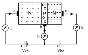
Anyhow, this is what an NPN transistor looks like:

Transistor

so as you say, the collector-base junction is reverse biased and no current flows.

Although it isn't clear from the picture, the base is very thin and lightly doped so the hole density is quite low. As soon as you apply a voltage to the base, electrons flow from the emitter into the base and start combining with holes. These electrons can then cross the base-collector junction and a current flows between the emitter and the collector. As you increase the base voltage further more electrons flow into the base from the emitter, so more flow into the collector and more current flows. This is how the small current between the emitter and the base can control the much larger current between the emitter and the collector.

A PNP transistor works the same way but in reverse.

$\endgroup$
2
  • $\begingroup$ You say that the base is lightly doped... isn't it also true that the collector and emitter are similarly lightly doped, albeit with a differential material (that makes it n-type)? I mean, my expectation is that the hole density in the base is the same as the extra electron density in the others. I'm wondering if there's some more sophisticated picture that I don't have the background for, or if I'm just reading too far into that. $\endgroup$ Commented Jan 8, 2013 at 17:55
  • 1
    $\begingroup$ As I recall, the collector layer is moderately doped and the emitter layer is heavily doped. $\endgroup$ Commented Jan 8, 2013 at 18:06
3
$\begingroup$

From a first approximation, the depletion zone of a reverse-biased diode is simply an insulating region. But this doesn't explain the collector junction of a transistor. We need to look at this insulation-effect in more detail.

In truth, a depletion zone does not block the motion of any charge carriers found there. Instead, there's (usually) no significant carrier population there in the first place. A depletion zone is an insulator like an empty vacuum: a voltage placed across a vacuum will produce zero current, showing that a vacuum is insulating ...yet any charges injected from outside would easily flow.

In a reversed diode, electrons from the n-doped side might invade the depletion zone. But they'd be forced back by the strong e-field in that zone. The same thing happens if holes from the p-doped side should invade the depletion zone: they're pushed back again.

But what if we dumped a bunch of electrons into the p-doped side of our diode? Sure, many would be swallowed up by the holes there. But some would pour into the depletion zone, where they'd be strongly forced across the junction and into the n-doped side. (The larger the reverse-bias voltage, the faster those charges would move.) So, dumping charges into the wrong side of a reversed diode will cause a large current.

And that's exactly what transistors do: in an NPN transistor, the Emitter region dumps large numbers of electrons into the p-doped Base. From the viewpoint of the CB junction, those electrons are on the wrong side of that diode. A few are swallowed by holes, but the majority wander through the Base region, and make it all the way over to the Collector's depletion zone. If they touch it, it grabs them and accelerates them with the full Vcb voltage-field, flinging them into the collector region. (Their large K.E. causes the Collector to heat up.)

So, heh, a BJT is much like a vacuum tube triode, where the Collector region is like a positively-charged metal plate, and the depletion zone of the Collector junction is like a vacuum with a large voltage placed across. And even worse[*], with NPN transistors, if we force the initially-positive Vbe to become more and more negative, it turns off the electron flow, just like a Grid electrode does.

.


[*] Worse for those who dislike the idea that BJT transistors are like FETs and vacuum-triodes: they behave as transconductance components, with output current controlled by a voltage signal.

$\endgroup$
6
  • $\begingroup$ That is the best explanation I have ever seen. The re-phrasing of depletion layer as more of a "vacuum" rather than a "perfect insulator" is very helpful! $\endgroup$
    – akhmed
    Commented Jun 19, 2017 at 17:43
  • $\begingroup$ Where is the CE junction? $\endgroup$
    – Willwsharp
    Commented Nov 27, 2019 at 0:21
  • $\begingroup$ @Willwsharp it's just above the Golgi Complex. $\endgroup$
    – wbeaty
    Commented Dec 2, 2019 at 11:14
  • $\begingroup$ @wbeaty I'm not sure what that means, could you explain further please. $\endgroup$
    – Willwsharp
    Commented Dec 2, 2019 at 14:39
  • $\begingroup$ @Willwsharp your humorous comment needed appropriate response. (There is no CE junction of course. Typo is now fixed. And, to find out about obscure terms in microbiology, google.) $\endgroup$
    – wbeaty
    Commented Dec 3, 2019 at 4:05
0
$\begingroup$

In reverse bias , minority carriers can contribute current not majority carriers.So during reverse bias of the collector - base diode the electrons acts as minority carrier in npn transistors and because of that current conduction takes place.

$\endgroup$
1
  • $\begingroup$ A diode is a device with two conductors. If you break emitter conductor of a bipolar transistor, then you’ll obtain a “collector–base diode”, but lose a transistor. While it is still a transistor, the thing is called the C–B junction or transition. $\endgroup$ Commented Oct 24, 2014 at 20:14
-1
$\begingroup$

Simply put, and speaking about a NPN. The base emitter junction is forward biased to allow current to be injected into the emitter. The transistor uses this small injected current and amplifies it in the current that flows from Collector to Emitter. The mechanisms for that are complicated and I won't cover it. But in essence if you also want the base collector junction to be forward biased then the amplified current would also flow into the base. You wouldn't have a transistor then as these currents need to be kept seperate.

$\endgroup$
-1
$\begingroup$

The collector base junction is reverse biased so that it attracts majority charge carriers and this jonction offers a high resistance to the current(as in rev. PN junc diode)

$\endgroup$

Not the answer you're looking for? Browse other questions tagged or ask your own question.