tl;dr I simply can not understand the orientation of the upper 45° optical surface.
In the semiconductor industry optical metrology is widely used to measure a combination of thin film thicknesses via interferometry and 2D/3D nanostructure dimensions not by optically resolving them but by recording their spectral response over a wide range (near UV to near IR) and comparing the spectra to rigorous EM models (based on dispersion models for the materials) as well as recorded spectra from reference samples. This allows the throughput necessary for manufacturing that high resolution scanning electron microscopes struggle with since they require at least a partial vacuum at the sample for direct imaging of nanometer-scale structures.
Scatterometry and Optical Critical Dimension Metrology based on polarized reflectance spectroscopy and/or ellipsometry is described further in (just for example) Optical Critical Dimension Metrology for Semiconductor Manufacturing (Vacuum Technology & Coating, Sept. 2021, pp 33-37)
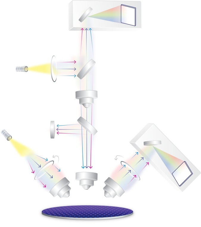
But the diagram below is driving me crazy because I can not understand how the optical system depicted can work.
On the sides are the two arms of a variable angle spectroscopic ellipsometer - the high NA objectives subtend a significant range of angles and the rotating polarizers are indicated. I'm not asking about this system. One arm has a broadband light source and the other has a spectrophotometer.
There is also a second optical system normal to the sample surface. It has its own light source and spectrophotometer. There are two stand-alone optical elements that are shown with surfaces at 45° to the optical axis. (a third is integral to the spectrophotometer)
The lower one appears to dead-end to the left and that's probably a camera for alignment - the system only works on certain repetitive/periodic structures that can be modeled, sometimes in memory areas of a chip, or on dedicated test structures in the scribe lanes between chips. By necessity these are sometimes small and the system must align the optical spot to them.
Thus I assume this represents a beam splitter or half-slivered mirror of some sort.
The other is associated with the broadband light source, and the thin element between the light source and the 45° element that looks just like the other two linear polarizes may indeed be a polarizer (sans arrow indicating rotation) or just a collimator lens.
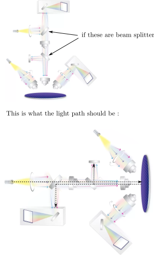
But what confuses me is the orientation of this 45° upper optical surface (not the one integral to the spectrophotometer); it seems to be able to send the light directly up into the spectrophotometer, but not towards the sample.
I'm assuming that if the normal incident light never reaches the sample, then it can't be measured.
Question: Am I missing something? Are there broadband beam splitters with surfaces in this orientation that can send the light downward? Could the diagram be essentially "wrong"? How do normal incidence reflectometers work (optically) and why can't I understand the upper beamsplitter in this diagram?
Source: https://www.novami.com/nova-technology/spectral-interferometry/


