0
$\begingroup$

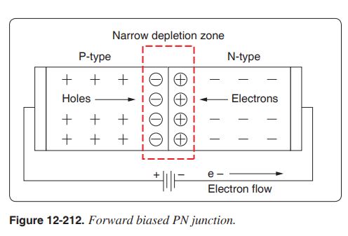
The text from book is:

    1. Electron leaves negative terminal of the battery and
       enters the right end (N-type material) of the diode.
    2. Electron then travels through the N-type material.
    3. The electron nears the junction and recombines and
       becomes a valence electron.
    4. The electron now travels through the P-type material as a valence electron.
    5. The electron then leaves the diode and flows back to
       the positive terminal of the battery. 

enter image description here

The electrons from N-type material combines with the positive ions in junction. And they become Valence electrons. But how do they cross the negative part of junction? Will not the electrostatic repulsion let it not cross it?

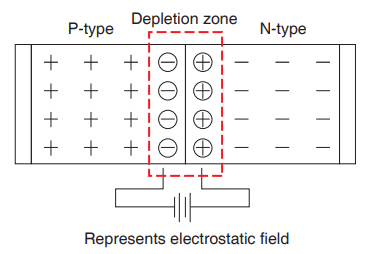
One solution I believe if my doubt is correct is that, the barrier electric field produced by depletion layer behaves like a battery with opposite polarity.

enter image description here

And thus the valence electron crosses because of the field and reaches to P-type material.

But this produces a contradiction when forward current keeps flowing and the depletion layer, so the barrier field, reduces after some time. Please correct me.

$\endgroup$
3
  • $\begingroup$ Sometimes conduction in the p-type is described as conduction by holes. Holes are created at the connection to the p-type and travel towards the junction. Electrons also travel towards the junction in the n-type. They meet and the electron fills the hole, at the junction. On the other hand putting electrons into the p-type just fills holes, making them not available to conduct, so the resistance is very high. $\endgroup$
    – Peter
    Commented Sep 12, 2020 at 10:39
  • $\begingroup$ @Peter This is what leads to formation of depletion layer. The free electrons from valance band of N-type goes to the hole of P-type and becomes negative ions, while the place it left becomes a positive ion. Which produces an electric field. The question is about: What if an another valence electron is sent in this positive ion section, how it will cross the negative ion section? $\endgroup$ Commented Sep 12, 2020 at 11:01
  • $\begingroup$ The short answer is "with great difficulty"! Adding electrons to the p-type merely fills more holes, ie there are fewer places for valence electrons to move into. In the n-type, removing electrons obviously makes it less conducting. The effect is to widen the depletion layer. Of course if the applied potential/field is great enough electrons will be pulled out of the holes, and the diode has broken down (eg Zener diode). $\endgroup$
    – Peter
    Commented Sep 12, 2020 at 11:23

2 Answers 2

1
$\begingroup$

"The electrons from N-type material combines with the positive ions in junction. And they become valence electrons. But how do they cross the negative part of junction? Will not the electrostatic repulsion let it not cross it?"

The first sentence above is incorrect. The electron does not recombine with a positive ion. Instead, the electron falls to a missing state in the valence band (it recombines with a hole). What your text calls "becoming a valence electron". This is a culmination of the two processes:

  1. holes moving to the junction from the left (and thus a net valence electron moving right from the junction to the left hand contact).
  2. electrons moving to the junction from the right.

When the electron and hole recombine in and near the depletion region they have completed the motion of one net electron moving from the right contact to the left contact. These electrons and holes move across the junction by diffusion. The driving force for diffusion, the large gradient in concentration between n and p under forward bias, is much stronger than the opposing electric field of the junction.

I would urge you to discard this text. It's teaching the version of semiconductor physics that says "there are no such things as holes". It also completely ignores diffusion in the explanation. Your question clearly points out how much confusion this approach can have.

We have had an excellent theory of semiconductors since William Shockley's seminal book:

Electrons and holes in semiconductors : with applications to transistor electronics, William Shockley, New York : Van Nostrand, 1950.

$\endgroup$
1
$\begingroup$

I think DrFalcon addressed the issue quite accurately, but I thought I would add further context as to what happens under different conditions of external electric fields.

Per PVEducation, see the following electric field plot along the axis of the junction:
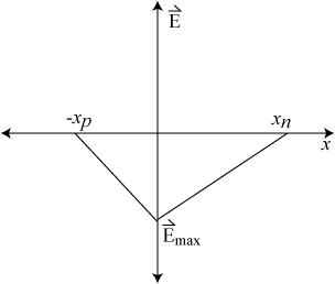
enter image description here

Since the electric field is defined for a positive point charge, holes will move to the p-type region (-x), and electrons to the n-type region (+x). This is without external fields applied. What's critical to understand here is that if a junction is disconnected and isolated, no internal or intrinsic electric field exists outside the depletion region due to the p- and n-type regions being electrically neutral (and electric field lines must always align/begin/stop). Diffusion is the predominant mechanism, so electrons/holes will not spontaneously cross the depletion region.

If external fields are applied, as in your textbook's example, these fields add and introduce different plots:
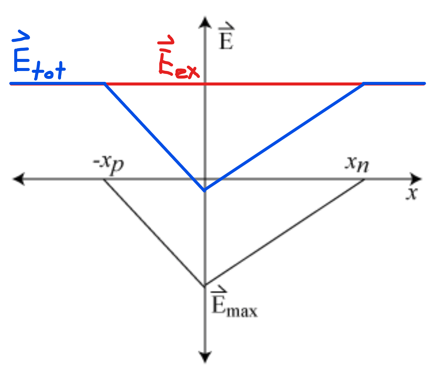
enter image description here

An electric field is present outside the depletion region.

If the external electric field (applied in the opposite direction) is less than the internal one (above), then there will be points inside the junction when the total electric field is 0 and neither holes nor electrons will be able to fully cross the junction and establish drift current. There will be a collection of charges at and near the crossing points within the junction.

If the external field is greater than the internal one, then null points cease to exist and the entirety of the junction allows electrons to flow, even across the depletion region:
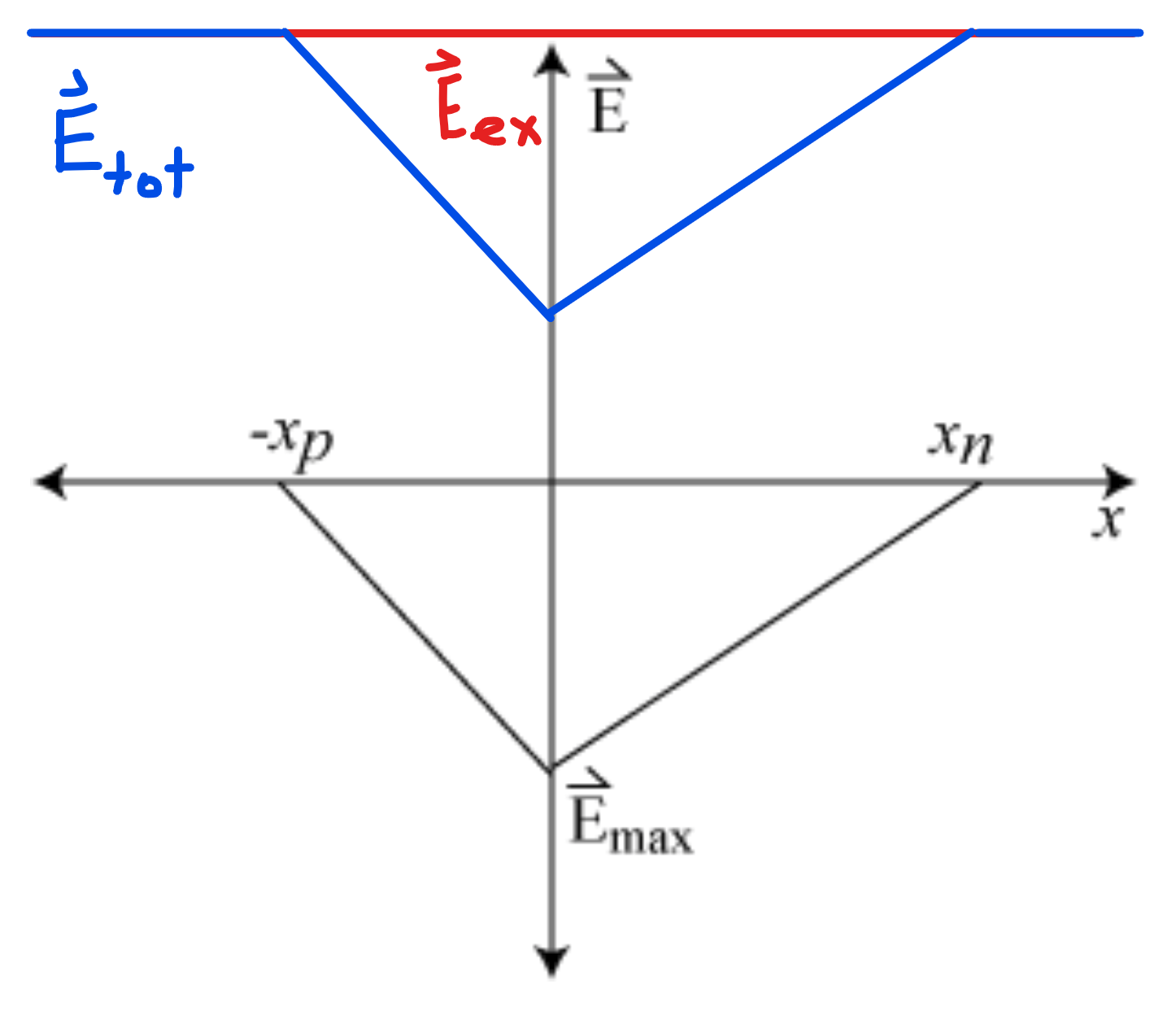
enter image description here

So, your battery or applied voltage source needs to overcome this built-in voltage of the PN junction, whether diode or BJT or whatever, in order for electrons to fully cross the depletion region and establish current.

The positive and negative portions of the depletion region aren't fixed, however, as others have said. They shrink or expand under forward or reverse bias, as can be seen in this Electronics Tutorials article:
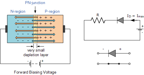
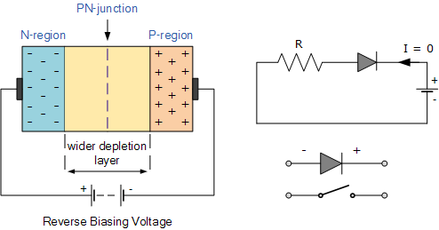
enter image description here

enter image description here

This corresponds to different slopes of the electric fields in the pictures above.

I don't believe that the depletion regions under extreme forward or reverse biases can ever fully disappear (infinite current?) or fully encapsulate the junction (infinite current?) because real systems always have parasitic resistances that limit current to some amount (before energy exchange between excited electrons and travel media becomes so much that molecular bonds start to break down and the material degrades). Maybe others have explanations for these situations, even before avalanche behavior under either bias.

Hope this clears anything else up!

$\endgroup$

Your Answer

By clicking “Post Your Answer”, you agree to our terms of service and acknowledge you have read our privacy policy.

Not the answer you're looking for? Browse other questions tagged or ask your own question.