1
$\begingroup$

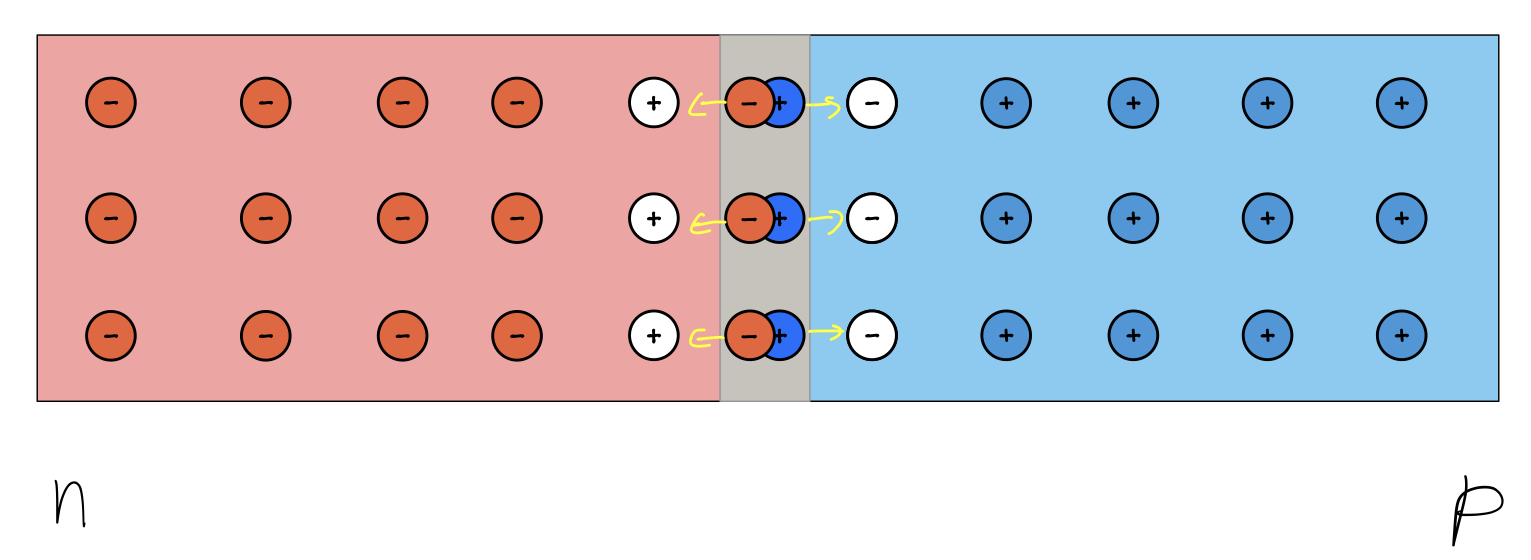
I have a p-n junction diode(For simplifying,consider it as a stack of array of spherical atoms arranged in a cuboid of length L).Now divide the cuboid into 2 half cuboid each of length L/2 and this partition wil be p-n junction .Consider the event when depletion region is already formed.Now the atoms just touching the junction on one side will be positively charged(n region) and the other side will be negatively charged(p region).Suppose we have 2 or 3 layers of such atom each in both region.

Now my doubt is what we mean by width of depletion region? I know how an electric field is set up between two plates of charges but this condition is somewhat different as in each region we have something like,say, a rectangular box of positive charged atoms and similarly a box of negatives.I am unable to think of depletion width and so unable to visualize the extent of electric field in depletion region.Someone please help. Edit: I just entered a picture to describe my doubt clearly .As we can see two layers of positive charged atoms and in same way two layers of negatives.If we describe depletion width to be 4 times the atom width(in my example)I don't get it as electric field between two one positive-one positive layer is different from one positive -one negative layer.The problem arises with potential barrier.With such description how can we say that V=E times depletion width.(https://images.app.goo.gl/QqcuVB9Sbea6j4sr9)

$\endgroup$
2
  • $\begingroup$ I can't quite understand the question. I can comment that you have made no mention of electrons and holes, and neither does your figure. Perhaps that omission is a the root of your difficulty. The question of the properties of the depletion region is practically identical to the question: what's happened to the electrons and holes. $\endgroup$
    – garyp
    Commented Feb 2, 2020 at 15:34
  • $\begingroup$ @garyp In my doubt I am talking of depletion region which is devoid of electrons and holes you mention. $\endgroup$
    – Sharad1
    Commented Feb 2, 2020 at 16:15

1 Answer 1

0
$\begingroup$

First thing to note is that the junction as a whole is neutral. But in the p-doped region there is an excess of holes and in n-doped, am excess of electrons. These excess “things” are charge carriers because some of them can move/hop in the material (statistically some will contain enough energy to be in the conduction band).

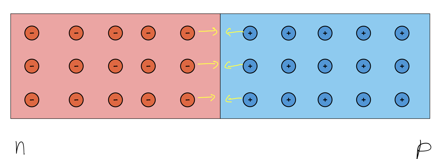
Consider the initial condition:enter image description here Where the left portion has more electrons than the right portion. This means that the electrons near the junction would begin to move to the right. This is known as diffusion current. It is dependent on the carrier concentration. This would mean that the electrons and holes would meet at the junction and neutralise each other. This is called depletion region. enter image description here However, in doing so, they would leave the opposite charge behind. This would attract the charge carriers back (since the carriers in the depletion region are the closest). Now the strength of this attraction is dependent on material properties. Thus the width of the depletion region is dependent on the balancing of these two opposing factors.

$\endgroup$

Your Answer

By clicking “Post Your Answer”, you agree to our terms of service and acknowledge you have read our privacy policy.

Not the answer you're looking for? Browse other questions tagged or ask your own question.