4
$\begingroup$

I am trying to get a clear picture of the valence band, conduction band, and the band gap. Now I've been researching it for a little while now and understand most of what's going on. I'm still a little confused about some specifics though, so if you could please address the following, that would be great!

My favorite description thus far has been

"The most important aspect of semiconductor bandstructure may be summarised as follows; at absolute zero the highest completely filled band (the valence band) is separated from the lowest empty band (the conduction band) by an energy gap or band gap Eg of forbidden states. Therefore the material does not conduct electricity at T = 0."

So from this description I have a pretty clear idea of what the valence band is (with the supplement of a few diagrams). Also, I know the conduction band is above the valence band in terms of energy, and is where electrons are free to roam the material as conduction electrons. My problem is where this "conduction band" is physically. It seems like there should be some allowed state, where if you just excite one electron you pass into that new state. From the above description, it seems to say some of these states are "forbidden", and that is my main question resides. Where is this conduction band, what determines its range (an example would be fantastic), and how do we determine what is necessarily a "forbidden" state?

Thanks =)

$\endgroup$
2
  • $\begingroup$ My problem is where this "conduction band" is physically, I could be wrong but, I suspect that you're trying to place this "band" in physical, i.e., configuration space. The conduction band is a range of (allowed) energy. $\endgroup$ Commented Nov 13, 2013 at 3:33
  • $\begingroup$ Well i know it's not an object and that's it's an energy range, I'm more looking for what the physical grounds for this energy range is, like what physically causes the conduction band to have this given range $\endgroup$ Commented Nov 13, 2013 at 4:34

1 Answer 1

7
$\begingroup$

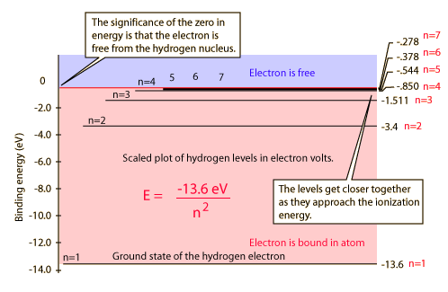
Take the solutions of the potential problem of an atom and look at the energy levels.

hydrogen energy levels

Between the n=1 energy level and the n=2 energy level there is a forbidden gap in energy, i.e. you will not find the electron of the hydrogen atom there. Note the thick line for large n where the energy gaps become so tiny leading to a continuum , i.e. an energy "band" where one can find the electron when measuring its spectrum.

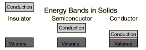
One can always model the collective potential of many atoms in bulk. New energy levels appear due to this collective potential in which the electrons see the whole lattice and not just the parent nucleus, depending on the material.

bands

Instead of having discrete energies as in the case of free atoms, the available energy states form bands. Crucial to the conduction process is whether or not there are electrons in the conduction band. In insulators the electrons in the valence band are separated by a large gap from the conduction band, in conductors like metals the valence band overlaps the conduction band, and in semiconductors there is a small enough gap between the valence and conduction bands that thermal or other excitations can bridge the gap. With such a small gap, the presence of a small percentage of a doping material can increase conductivity dramatically.

The gaps, where electrons are "forbidden" arise because of the collective potential and solutions it allows . One can intuitively understand why bands form, because of the collective potential of a large number of atoms and the uncertainty principle due to the quantum mechanical nature at this level: The lattice is vibrating due to thermal motion and the levels get smudged :).

$\endgroup$
0

Your Answer

By clicking “Post Your Answer”, you agree to our terms of service and acknowledge you have read our privacy policy.

Not the answer you're looking for? Browse other questions tagged or ask your own question.