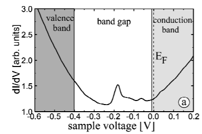
I think it is better to really think physically about how energy band structures determine the electronic transport.
First, let's answer the question, which electrons participate in the electronic transport of the material? Well, transport requires some empty available energy levels throughout the material in which electrons can move "freely". The electrons that can be excited into these empty states are the highest energy states, i.e. the electrons closest to the Fermi level. So indeed, the electrons close to the Fermi level determine the electronic transport properties.
Secondly, we must ask the question, where is the Fermi level located. If it is located in an energy gap, then the electrons will be located in the valence band, the closest energy band below the Fermi level. Electrons can be excited and overcome the energy gap. Depending on the size of the energy gap we speak of insulators or semiconductors. However, if your Fermi level lies inside an energy band such that there are sufficient available (non-occupied) energy states above the Fermi level which lie still inside the energy band. Well, in that case, electrons can be easily excited into these available states where they are considered as being "free carriers". So in this case, we speak about a metal.
So to answer the question whether we need overlap of valence and conduction band. Well, when $E_F$ is located in the above energy band (in your figure), we will say that the valence band becomes to some extent the part below your $E_F$ (so no longer the one from the figure) and the part above is the conduction band to some extent, and in this way there is an overlap. But don't pin yourself too much on these notions. Keep in mind the physical intuition from above.

