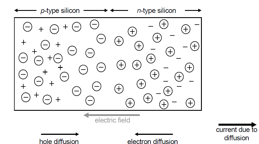
Why electric field pointing to left? (The middle area is depletion region.)
(This is without any external electrical voltage applied.)
It is simple than you think. For a few centuries (after Faraday gave the concept), we've assumed Electric field lines to start from positive charges and terminate at the negative ones. So, the direction of electric field (given by the field lines) flows from Positive ions $\rightarrow$ Negative ions.
It's all based upon the doping mechanism. I'll try to explain it somewhat.
When donor and acceptor atoms are doped into an intrinsic semiconductor crystal (silicon, in your case), the free electrons and holes (absence of electrons) in both the regions start to recombine with each other (by diffusion). Within a short period of time (we can't notice this though), a region is formed which doesn't contain any mobile charges. This prevents the recombination of electrons and holes further.
Once the donor atoms lose their free electrons, they become positive ions and the same happens for acceptor atoms. These ions are immovable and this also prevents the to or fro motion of mobile charges on either side of the depletion region.
Hence, this was given a name potential barrier. Once the charges have got enough energy to cross the barrier potential ($\text{0.7 V}$ for Silicon, I think so - from high school experiments), the barrier gets increased further. But, that doesn't happen naturally. The increased or reduced size of the depletion region totally depends on the bias (forward or reverse) of the PN-diode.
Doped silicon is an electrically neutral material. When the electron-hole pairs form in the depletion region they actually create an electric field because there are actually more electrons in the P-type silicon in the depletion region.
Note that the electron-hole pair formation allows the system to be at a lower total energy, even with the electric field that it creates...