5
$\begingroup$

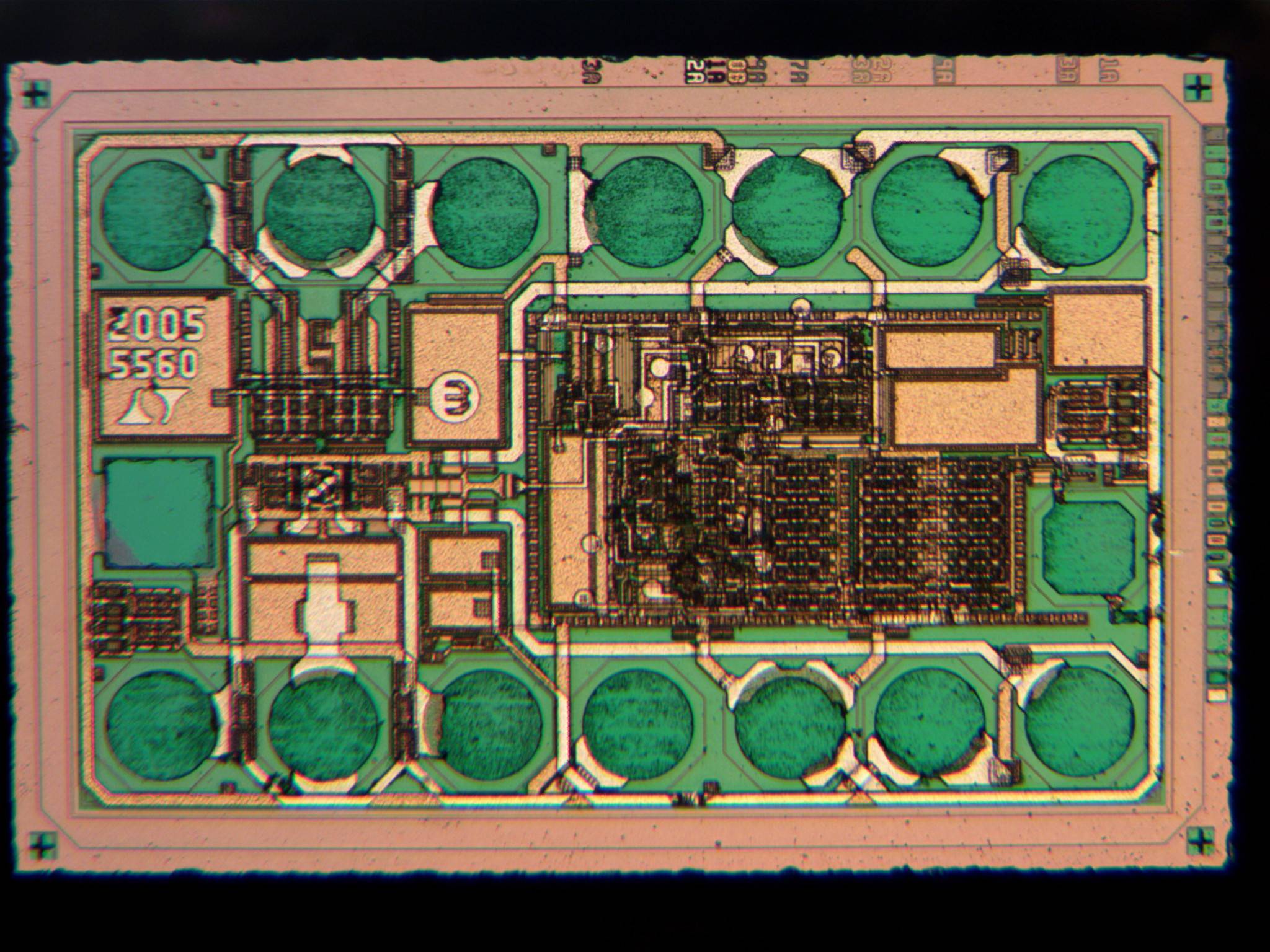
I am currently trying to improve my silicon microphotography. To provide context: this is what I get with a 10x epi plan objective¹:

enter image description here

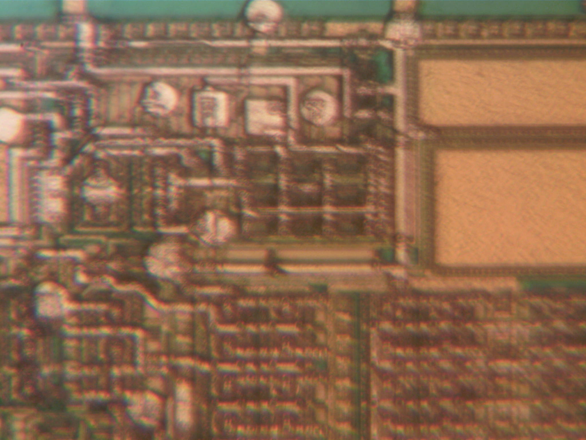
This is what I get with 40x epi plan objectve with NA=0.65:

enter image description here

I can get very good resolution with a 100x epi plan oil immersion objective with NA=1.25, but the magnification is too large: there's over 4 times more movements I have to perform to traverse the entire IC and the stage is not very high-quality, making that harder.

Because of the above, my understanding is that the 40x objective has an NA which is too small for my goals. I tried to find a 40x epi plan objective with NA>=0.95 (immersion or not), but it appears that there is no local supplier. After selecting for NA and magnification in range of 40x-60x, it appears that I can get:

  • 60x non-epi apochromatic water immersion with NA=1.0
  • 40x non-epi apochromatic with NA=0.95

Unfortunately, the supplier does not accept returns ever.

The question is: would a non-epi objective work with epi illumination? My understanding is that epi objectives differ in that they 1) have additional antireflection coatings 2) are not corrected for 0.17mm specimen cover glass.

More generally, how would one select an objective given the constraints that I have?

¹ I know it's overetched, alright?

$\endgroup$
12
  • $\begingroup$ Honestly, I think you are optimizing the entirely wrong end of this. If you can get good images with the 100x epi at NA=1.25, that's the way to go. The remainder is a software problem for the stitching of the images, which is essentially solved. $\endgroup$
    – CuriousOne
    Commented Sep 17, 2015 at 19:58
  • 1
    $\begingroup$ @CuriousOne For this chip, which is smaller than 1mm, I will have to take 14x14x3=588 pictures manually: one for every one of the three layers of it. That's a lot of work. Most of the chips I'm interested in are substantially larger, which makes it downright intractable. With less magnification, I don't care about layers because they're all in focus enough for my purposes. $\endgroup$
    – Catherine
    Commented Sep 18, 2015 at 0:11
  • $\begingroup$ At which point I have to throw my hands up in the air and simply admit that I believe in my heart that what you have is not a physics but an economics problem... how to get better equipment that gets the job done. It seems to me that a modern confocal microscope should be more than capable of doing what you need... the only question is where you can get the $100k for a modern confocal microscope. Is that halfway correct? $\endgroup$
    – CuriousOne
    Commented Sep 18, 2015 at 0:17
  • $\begingroup$ What is epi-illumination? Is this Kohler illumination were the objective its self is used to flood the sample? Comment: you should think about changing supplier! I've had great experience with asking Thor Labs for technical support when selecting the correct optical components. Worth a try. $\endgroup$
    – boyfarrell
    Commented Sep 18, 2015 at 10:07
  • 1
    $\begingroup$ @boyfarrell Epi-illumination: correct (although I've never heard it described like that before). Changing supplier: I'm an amateur in what you'd call a "third-world country". My supplier here is one step above a flea market (or eBay, but eBay is an order of magnitude more expensive). Frankly I was still shocked to learn they neither accept returns nor understand what they sell, but that was not completely unexpected. $\endgroup$
    – Catherine
    Commented Sep 18, 2015 at 10:58

1 Answer 1

1
$\begingroup$

This will be an answer for future readers, based on my experience at ZeptoBars.

For analog chip microscopy (like you have here) NA 0.3-0.45 should be well enough to reach sharp image where all chip features are clearly visible. If you are not getting sharp image - issues could be at:

  1. Too small illumination aperture (typically nearly all EPI-illuminated microscopes has adjustable apertures). You need to increase aperture as long as image is getting brighter and then a little reserve.

  2. Incorrect lens type: Infinity vs 160/180 tube. No good/easy fix other than replacement.

  3. Flawed lens (non-symmetrical aberrations often point to that), and unfortunately on the image I see vertical chromatic tail which hints on misalignment somewhere in the lens (if this color separation is visible only with this lens)

  4. If you are using 0.5x camera adapter - it is often largest contributing factor for quality reduction. You can get passive 1x adapter to check ultimate image quality. There are good 0.5x adapters, but good way forward is camera with larger sensor (at least 1", not more than APSC) which would allow to see same magnification with 1x adapter.

  5. Incorrect cover glass thickness / immersion.

General notes:

  • Do not increase NA when not needed. It is exponentially harder to work with large panoramas at high NA due to tight focus requirements. >0.65 you require full automation. Often 0.25-0.3 or even 0.16 is enough.
  • For non-transparent speciments epi/non-epi lens does not matter much, if other optical specs are met (tube length, cover glass, immersion). I've noticed no difference in epi-rated vs biological low-magnification lenses in as-designed conditions. There might be difference in fluorescence e.t.c, might be slightly lower contrast - but this is outside of the scope, all this would hardly affect normal bright-field image.
  • You definitely do not want dark-field illumination for chips, unless you are looking for dirt and defects.
$\endgroup$
1
  • 1
    $\begingroup$ Wow, @BarsMonster himself!! I'm honored. I have since lost most of my microscopy setup in a series of cross-border moves, but I will definitely heed this advice whenever I get back into it. $\endgroup$
    – Catherine
    Commented Oct 23, 2023 at 14:15

Your Answer

By clicking “Post Your Answer”, you agree to our terms of service and acknowledge you have read our privacy policy.

Not the answer you're looking for? Browse other questions tagged or ask your own question.