4
$\begingroup$

I'm a college student studying semiconductors. I can't understand what is happening inside the materials when two or more different materials are in contact. Can I get some help?

So, basically at thermodynamic equilibrium, the Fermi level of all materials should be the same. Yes, I understand that, because the electrons of each material will tend to move to a lower energy level, ultimately reaching equilibrium.

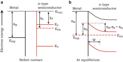
However, in metal & n-doped semiconductor junctions, as you can see in the figure below, the Fermi level of the semiconductor is higher than that of the metal. Therefore, I assumed that electrons will flow from the semiconductor into the metal. If that's the case, shouldn't metal's Fermi level increase? Why does the Fermi level of semiconductor change only, instead of both materials? Also, I learned that at the surface of each materials, the charges pile up, creating a barrier (Schottky barrier). However, if electrons migrate into metal, which has high conductivity and freedom of movement of electrons, in what way does charges pile up?

figure of metal-semiconductor junction

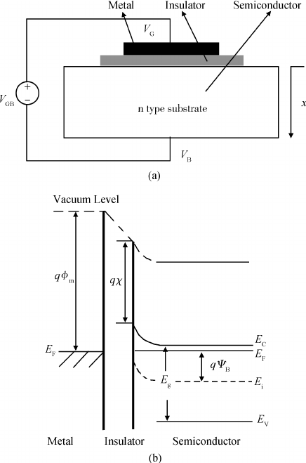
My second question features the MOS structure. As you can see in the figure below, all the materials are in contact, reaching a equilibrium. However, the oxide layer acts as an insulator, forbidding electron movement through the material. In this situation, in which mechanism does the Fermi level reach equilibrium throughout all materials?

figure of MOS structure

Thank you.

$\endgroup$

1 Answer 1

3
$\begingroup$

Why does the Fermi level of semiconductor change only, instead of both materials?

In principle, the Fermi level changes in both materials. However, the metal has a lot more electrons than the semiconductor does. In a semiconductor, only dopants contribute electrons, and dopants make up a small fraction of the total number of atoms. In a metal, basically all atoms contribute electrons. So, shifting the Fermi level in the metal takes a lot more energy than shifting the Fermi level in the semiconductor, and to a good approximation, the Fermi level in the metal doesn't move; the Fermi level in the semiconductor does. This is is just an approximation; the Fermi level in the metal does move a little, but it's such a small effect that it's usually ignored. (An exception is when you have a small amount of metal relative to the amount of semiconductor.)

in what way does charges pile up?

To get a constant Fermi level, the bands have to bend near the interface. This basically creates a potential well that the electrons fall into. (Arguably, cause and effect run in the opposite direction.)

In [a MOS structure], in which mechanism does the Fermi level reach equilibrium throughout all materials?

In practice, it doesn't reach equilibrium. (Unless you have a crummy oxide layer.) If you waited a really long time (sometimes on the order of years or even decades), eventually electrons would tunnel across the barrier (or be thermally excited over the barrier) and the Fermi level would equilibrate. So, MOS devices generally aren't in equilibrium; they're in a metastable state. This is basically how flash memory works: a structure similar to the gate gets charged up and takes so long to discharge that it can store information (i.e. retain its charge) for years or even decades. If you made a sufficiently thick, high-quality oxide layer, it would retain its charge effectively forever.

$\endgroup$
1
  • $\begingroup$ I think since in the picture the metal and the semiconductor are connected (and there is a VGB voltage), the electron can transport through this connection wire, and the VGB will result a fermi level difference of VGB. $\endgroup$
    – Dzhou
    Commented Oct 6 at 21:56

Your Answer

By clicking “Post Your Answer”, you agree to our terms of service and acknowledge you have read our privacy policy.

Not the answer you're looking for? Browse other questions tagged or ask your own question.