According to band theory, at $T=0\ \text{K}$ the Fermi level of an intrinsic semiconductor lies in between the valence band and the conduction band, while in the case of an insulator it lies near the valence band. Then why do we say that intrinsic semiconductors behave like insulators at $T=0\ \text{K}$, even though they both have different positions of the Fermi level?
1 Answer
Both semiconductors and insulators have band gap, which means that conductance cannot happen without exciting electrons from the valence band over the gap to the conduction band. For an insulator, this takes considerable energy, if it is even possible. Much more energy than is thermally available at room temperature. You can think of a semiconductor as an insulator which doesn't insulate very well. The gap is much smaller, so even though the valence band is filled (the fermi level is in the gap), it does not take much energy to excite electrons into the conduction band. In fact the electrons can be excited thus simply by thermal excitations at room temperature.
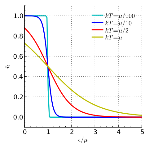
What happens at $T = 0$K? The distribution of electrons into different states becomes a step-function, with all electrons being below the Fermi level, and none above, see the figure below, where $\bar n$ is the how filled the energy level is from 0 to 1, $\epsilon$ is the energy and $\mu$ is the Fermi level ($T=0$K corresponds to $\lim_{\alpha \rightarrow \infty} kT = \mu/\alpha$).
In other words, all the electrons which were previously distributed loosely (e.g. the red curve) around the Fermi level (and thus possibly allowed to be in the conductance band) are now all locked strictly below the Fermi level (even more than the cyan curve). This means that as long as the Fermi level is inside a gap, at $T=0$K the material will be an insulator no matter how small the gap is.
(Graph taken from here.)

