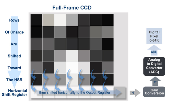
There are several concepts and issues going on here that are getting mixed together.
First the ADC;
An ADC (Analog To Digital Convertor) takes signal values in a certain range and converts then to a digital number. Let's run some numbers:
A N bit ADC will be able to represent 2^N states. So a 4 bit ADC can represent 16 distinct states, 8 bits => 256 States and a 12 bit convertor will give you 4096 states. By itself that tells you nothing, you need to know that going from a digital representation of say 533 -> 534 means that the input signal changed by certain amount. To keep the example simple I'm going to say that I have an input range from 0 Volts to 4.095 Volts on a 12 bit convertor, that means that when I have a digital number of 0 then I must have had 0 on the input. Let's also assume everything is ideal for now. With my sneaky choice of input range you can see that for every change in the ADC output digital number by one count then the input must have changed by 1 mV.
Why did I pick 4.095? Well a 12 bit convertor will have 4096 digital values that range from 0 to 4095 (2^N-1 when all the bits are set to "1"). So 4.095 Volts/4095 = 1 mv/count. That means that if you have a 3.567 Volt value on the output and it changes to 3.568 Volts ( 1 mV change on the input) then the digital number on the output should change from 3567 to 3568 digital number on the output from 110111101111 to = 110111110000 in raw binary.
Each of these binary steps are called an ADU (Analog Digital Unit) or Binary Number or Digital Count etc. etc. to keep it separate from the number of bits that the ADC has. This is to ensure that the relationship is in a linear range. If you start using "bits" then it is in a logarithmic range (2^N). The main reason these other names/units are used is that LSB's used to be used. What is a LSB? - it stands for Least Significant Bit, i.e. the zeroth bit in the digital number, which changes precisely in step with the ADU but using LSB (and the implied 'bit") is confusing. Imagine saying, " the ADC changed by 30 LSB's therefore the light flux must have changed by 3000 photons ". 30 LSB's really doesn't make sense, it is a mixing of terminology, so people are moving away from that. But that has meant that many different terms being used instead confusing again...
So you have a conversion from voltage into a digital number.
But you are collecting photons, where does voltage come from?
Next the Voltage conversion;
All image sensors at some point in the signal chain will convert the collected signal charge into voltage to interact with the outside world. This is always done using a capacitance and a buffer amplifier. This capacitor and the gain of the amplifier set the conversion from electrons into voltage as A/C_sense which is derived from the Q= CV equation. With C_sense = the sense node capacitance and A = gain of the buffer amplifier.
Next the photon conversion
When a Photon comes rattling into a pixel it has to make it into the photosensitive substrate, this interface is controlled by the fresnel equations and dictates how much light goes into the substrate based upon the indices of refraction and the various materials and AR coatings present (AR = Anti-reflection). This is known as the external QE (Quantum efficiency). Once in the substrate the photons are absorbed through it's depth and generate electron/hole pairs through the photo electron effect. Electric fields sweep the carriers into storage structures. The absorption depth and the depth of influence of the electric fields (these two depths may not be co-incident) are what determines the Internal QE. NOt every converted photon's carriers get collected.
These collected carriers (either electrons or holes) are brought to the sense node and converted into voltages. Where this conversion happens (carrier to voltage) is determined by the type of sensor, a CCD or CMOS image sensor.
The total conversion process;
(Photon flux) * (Integration period) * QE_external *QE_Internal * A/C_sense * ADC_conversion
Will give you units of Photons/ADU.

