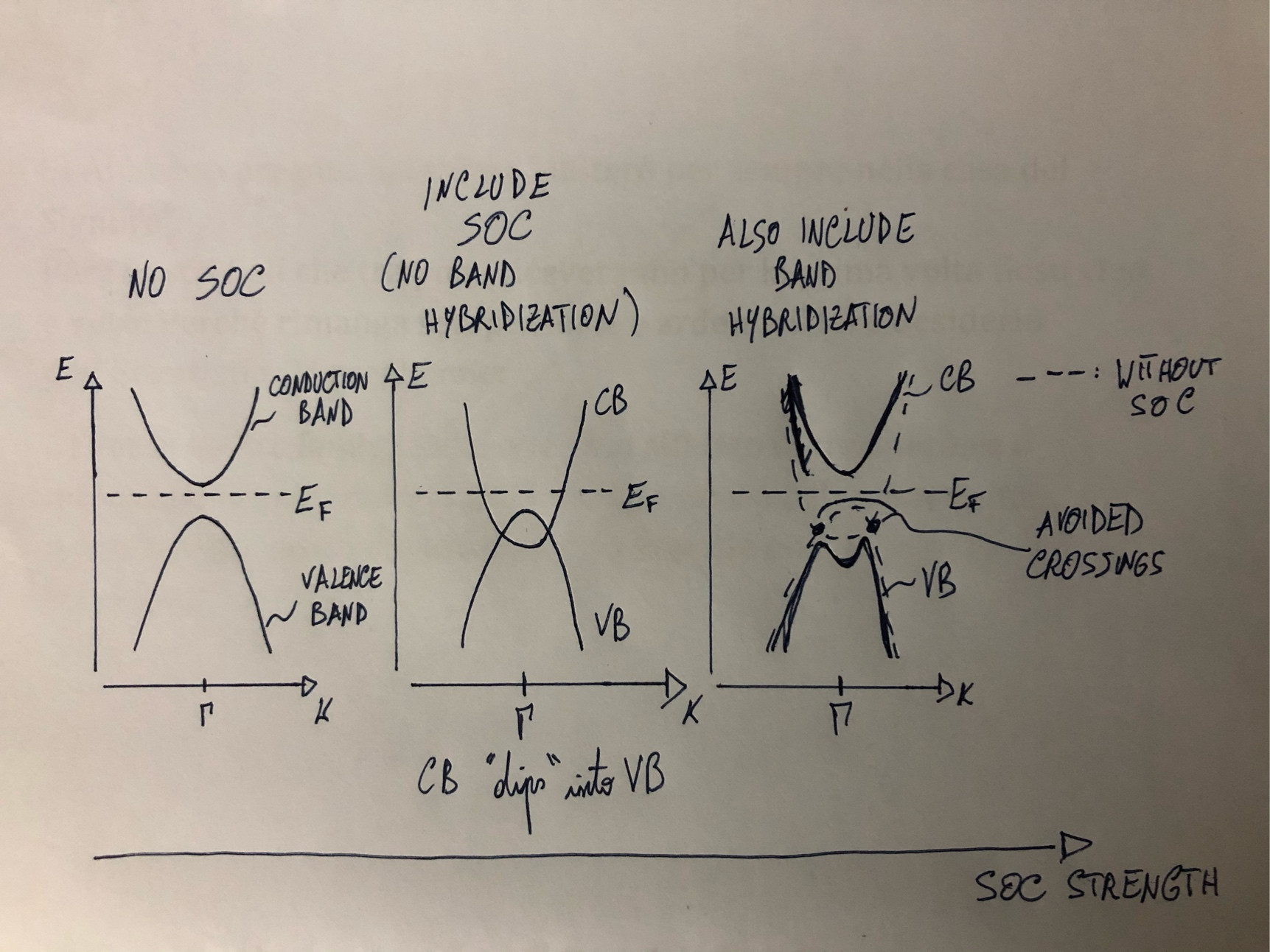
In this paper1 the following bandstructure of Bi$_2$Se$_3$ is shown:
In "a" they show the bands without Spin orbit coupling (SOC) and in "b" they include SOC. It is said that:
"Figure 2a and b show the band structure of Bi$_2$Se$_3$ without and with SOC, respectively. By comparing the two figure parts, one can see clearly that the only qualitative change induced by turning on SOC is an anti-crossing feature around the $\Gamma$ point, which thus indicates an inversion between the conduction band and valence band due to SOC effects, suggesting that Bi$_2$Se$_3$ is a topological insulator"
What is meant by the "anti crossing around the $\Gamma$ point after SOC is turned on?" Also before SOC is turned on there is no crossing between valence band and conduction band!?
And what is meant by the "inversion between conduction and valence band"? Am I supposed to see that conduction and valence bands are mirrored at the Fermi level (dashed line) when going from the left figure to the right? And why does this indicate that we have a topological insulator?
1 H. Zhang, C.-X. Liu, X.-L. Qi, X. Dai, Z. Fang & S.-C. Zhang, "Topological insulators in $\require{mhchem}\ce{Bi2Se3}$, $\ce{Bi2Te3}$ and $\ce{Sb2Te3}$ with a single Dirac cone on the surface", Nat. Phys. 5, 438–442 (2009).


 $\Gamma$ comes from the energy band you called conduction band in Fig. 2a, i.e. the band structure is inverted at this momentum." />