0
$\begingroup$

I was reading book On Semiconductor Physics By Donald Neamen,In page 176 He discussed semiconductor that is nonuniformly doped with donor impurity atoms.Now Here

The doping concentration decreases as $x$ increases in this case. There will be a diffusion of majority carrier electrons from the region of high concentration to the region of low concentration, which is in the $+x$ direction.Image
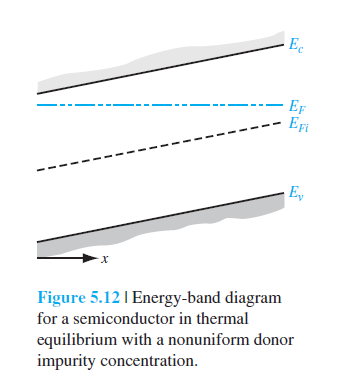
The fl ow of negative electrons leaves behind positively charged donor ions. The separation of positive and negative charge induces an electric fi eld that is in a direction to oppose the diffusion process. When equilibrium is reached, the mobile carrier concentration is not exactly equal to the fi xed impurity concentration and the induced electric fi eld prevents any further separation of charge. In most cases of interest, the space charge induced by this diffusion process is a small fraction of the impurity concentration, thus the mobile carrier concentration is not too different from the impurity dopant density.

The electric potential $\phi$ is related to electron potential energy by the charge ($-e$), so we can write $$\phi=\frac{1}{e}(E_F-E_{Fi})$$ {I din't understand ,How!} The electric fi eld for the one-dimensional situation is defined as $$\frac{dE_x}{dx}=\frac{1}{e}\frac{dE_{F_i}}{dx}$$ Can Some one Help me with this .

$\endgroup$

1 Answer 1

2
$\begingroup$

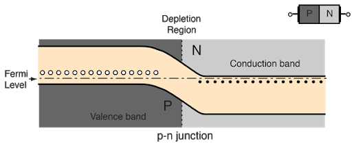
Check this image:

enter image description here

There are two things here.

First, see what is happening intuitively.

The P type has an excess of holes. The N type has an excess of electrons.

When they are put together, the extra holes go towards the N region and the extra electrons flow owards the P region.

However, a movement of electrons and holes is not as easy. If an electron moves, it's not just changing the concentration of particles; it is also changing the charge distribution.

The regions are initially neutral. If electrons go to the P region, negative charge starts getting accumulated there. At the same time, possitive charges are being accumulated in the N region. Only near the border in both cases.

So, if charges are accumulating in the border, there is obviously an electric field, from the possitive charges to the negative ones.

That's what is actually happening.


Secondly. The Fermi level.

The Fermi level of a P SC is next to the VB. The Fermi level of a N semicond. is next to the CB. But, if two materials are able to exchange charges, the Fermi level will authomatically be the same.

If the Fermi level has to be the same, the bands of the P region must go up and the bands on the N region must move down, so that the Fermi level is not constant (A straight line).


Third. The relation between the field, the potential and the Fermi level.

See the diagram. The bands are now in different energy levels.

There is an electric field through the border.

Of course, that electric field has an electric potential $\phi$ associated with it.

IF an electron wants to rise from the N region to the P region, it has to overcome an electric field, so it must overcome a potential difference.

The work done along that path is obviously $W=q\cdot \varphi$. And that work is the energy difference. Hence

$e\cdot \phi = \Delta E$

And that's where your formula comes from.

$\endgroup$
11
  • $\begingroup$ Why they change in fermi level in place of change of energy of electron from one side to other. $\endgroup$
    – Himanshu
    Commented Mar 19, 2020 at 11:20
  • $\begingroup$ Sorry, I don't understand your comment $\endgroup$
    – FGSUZ
    Commented Mar 19, 2020 at 11:48
  • $\begingroup$ $$\Delta E=E_F-E_{Fi}$$ How? I mean fermi energy is not the energy of electron. $\endgroup$
    – Himanshu
    Commented Mar 19, 2020 at 14:20
  • $\begingroup$ Also Why the fermi energy is same throughout the region. $\endgroup$
    – Himanshu
    Commented Mar 19, 2020 at 14:24
  • $\begingroup$ When you add donor levels, the Fermi level rises. A N-type SC has a higher $E_F$ than an intrinsic SC. That difference in energies is the one required to make a N semiconductor, and so it's the noe required to have the extra electrnos $\endgroup$
    – FGSUZ
    Commented Mar 20, 2020 at 11:29

Your Answer

By clicking “Post Your Answer”, you agree to our terms of service and acknowledge you have read our privacy policy.

Not the answer you're looking for? Browse other questions tagged or ask your own question.