3
$\begingroup$

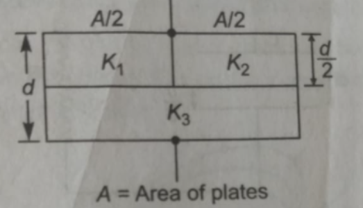
I am ripping my hairs trying to understand this answer, it is written that, for the following set up of two capacitor plates separated by distance $d$ and area $A$ with three dielectrics insert with constant $K_1,K_2$ and $K_3 $
2

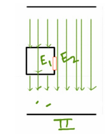
The electric field is not necessarily normal at the boundary joining the dielectric substances $K_1$ and $K_2$. If it is so, precisely, what would be the directions at points along the surface? Would all of the electric field vectors attached to these points be tilted differently or have same tilt amount?

It may be noted that this other answer on a different question says the opposite of this.

enter image description here

Picture sourced from mentioned answer

I had posted a question here on why it must be normal like so with no satisfactory answers.

The electric-static field is always normal to the surface of a conductor at the conductor. But you want to know why it is normal to the plates between the plates. Unfortunately, you won't find a rigorous mathematical proof of that, because it is not rigorously mathematically true. It is approximately true. It is true to a very good approximation, but it is not exactly true. The field lines actually bulge a little away from centre. The effect is small toward the centre of the plates, but gets larger toward the edges. This bulging is generally called "fringe" effects.

This again suggests it is normal but it contradicts the originally quoted answer.


Note

Assume area of plates is large relative to plate seperation

$\endgroup$
8
  • 4
    $\begingroup$ I think you should not expect people to explore different links you provided, trying to piece together what you are after. Please restructure your question in a self-contained manner here $\endgroup$
    – Cryo
    Commented Aug 30, 2021 at 21:48
  • 2
    $\begingroup$ You are still expecting people to go to the other links. Please condense your question, further. In case there are prior answers that do not satisfy you, please state them here. Coming back to the question. What is the aim of the question? Are you trying to solve for electric field, or estimate capacitance? What are the relevant approximations? Is it very large plates and very small gap? The reason I am asking is that if it is very large plates and small gap, then the gradient electric field near the boundaries is probably not important for the total capacitance. $\endgroup$
    – Cryo
    Commented Aug 31, 2021 at 12:00
  • $\begingroup$ I think you may find that proper answer requires solution of the relevant PDE for the field, however if there are approximations available, and if you are content with aggregate values, e.g. average gradient of electric field at the boundary, then you may be able to get away with analytically tractable approximate solution $\endgroup$
    – Cryo
    Commented Aug 31, 2021 at 12:07
  • $\begingroup$ Dear Cryo, thanks for the advice. I have edited the question and tried to make it more self contained. Have a look now @Cryo $\endgroup$
    – Brian
    Commented Aug 31, 2021 at 12:08
  • 1
    $\begingroup$ I have rectified that as well @Cryo $\endgroup$
    – Brian
    Commented Aug 31, 2021 at 12:10

2 Answers 2

4
+500
$\begingroup$

The boundary condition for the electric field states that the the tangential electric field on either side of the interface must be equal. This does not necessarily mean that it be normal to the interface. In the absence of free charges, the boundary condition for the normal part of the electric field is $$\epsilon_1E_{1\perp} = \epsilon_2E_{2\perp}$$

So what would happen in this case?

Let's consider two capacitors. They each consist of two plate seperated by a distance $2d$. They are both filled with two dielectrics, each dielectric taking up half the space between the conducting plates along the entire width, so that the thickness of each dielectric is $d$.

Consider now that capacitor 1 has dielectrics with permittivity $\epsilon_3$ and $\epsilon_1$ for the bottom and top dielectric respectivily. Capacitor 2 has dielectrics with permittivity $\epsilon_3$ and $\epsilon_2$ for the bottom and top dielectric respectivily.

For each, what will the voltage at the interface between the dielectrics be, if we set the top plate to a voltage V, and the bottom plate to 0V? Due to symmetry, the field lines are pointed straight down for both (ignoring fringing effects). Since the boundary condition for the perpendicular part of the electric field states that the electric flux density must be equal at the top and bottom, the voltage at the dielectric interface will be equal to $V\frac{\epsilon_1}{\epsilon_1+\epsilon_3} $ for capacitor 1 and similar for capicitor 2.

This means that the voltage at the dielectric interface will higher for the capacitor with the higher permittivity for the top dielectric.

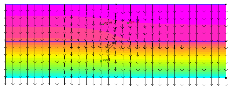
What then happens when the two plates of capacitors are connected and we get the geometry similar to the linked question? [2

Far from the interface between the two capacitors, the voltage levels will be $V\frac{\epsilon_1}{\epsilon_1+\epsilon_3} $ and $V\frac{\epsilon_2}{\epsilon_2+\epsilon_3} $. Close to the interface, there must be a transition region where the electric field points in the direction of decreasing voltage, towards the side of the capacitor that had the lower permittivity in the top region.

Quick simulation in femm of the described geometry: A complete picture is of course given by solving Poisson's equation for electrostatics with the appropriate boundary conditions.

$\endgroup$
1
  • $\begingroup$ >Let's consider two capacitors. They each consist of two plate seperated by a distance 2d. They are both filled with two dielectrics, each dielectric taking up half the space between the conducting plates along the entire width, so that the thickness of each dielectric is d. I think a pciture would help $\endgroup$
    – Brian
    Commented Sep 30, 2021 at 14:09
1
$\begingroup$

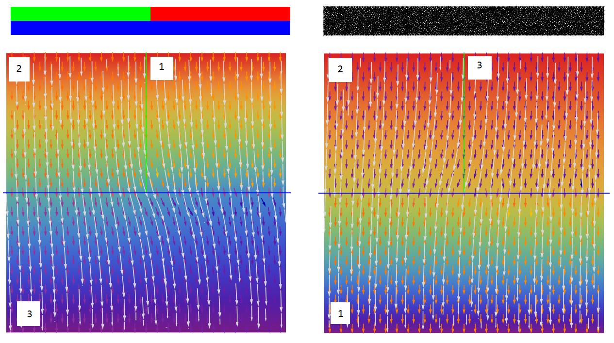
To illustrate nice answer by Cyrus, we simulate the capacitor with three dielectric plate with using finite element method implemented in Mathematica 12.3. In Figure 1 are shown lines of electric field for two variants of compound with relative dielectric constant in three regions: $K_1=2,K_2=1,K_3=3$ (left picture), $K_1=2,K_2=3,K_3=1$ (right picture). Figure 1

Note, that lines of electric field are bended from upper plate with higher dielectric constant to upper plate with lower dielectric constant.

$\endgroup$

Your Answer

By clicking “Post Your Answer”, you agree to our terms of service and acknowledge you have read our privacy policy.

Not the answer you're looking for? Browse other questions tagged or ask your own question.