1
$\begingroup$

I have recently started with my highschool course on semiconductors and after a general introduction as to what they are, I have graduated to the p-n junction. Almost all resources that teach the textbook course explain joining a p-type and n-type semiconductor in same way; the electrons and holes of n- and p-type semiconductors respectively diffuse due to their concentration gradient to the corresponding opposite side thus setting up a "diffusion" current. This creates a sort of charge separation$^1$ at the junction (why? Why don't the electrons that diffused from n to p combine with the holes there and kinda neutralise?) which keeps on increasing until it concentrates and then becomes constant.

Meanwhile, or as a consequence* (I'm not sure which, they don't explicitly say it), there is another current called drift current which is opposite to diffusion current where the electrons move from p to n under the charge separation created in $^1$ and holes vice-versa. This does not make sense to me. If the p side of junction had a negative charge, how could anymore electrons penetrate it to reach the other side and if we consider that this happens meanwhile, (while the diffusion current is concentrating to a constant value), then what is the driving force for the minority charge carriers to move (like that for majority was concentration gradient)?

Here's what I need to know:

a) if my explanation of how it works is correct regardless of what I make of it.

b) the answers to questions that I put in parentheses.

c) a resource to intuitively understand the topic.

d) an explanation of how the junction works if everything written above sounds gibberish to you.

$\endgroup$

2 Answers 2

0
$\begingroup$

Why don't the electrons that diffused from n to p combine with the holes there and kinda neutralise?

Conduction electrons in a crystal lattice (such as Si lattice) travel as waves. The number of electrons in the conduction band is small with respect to the atoms in the lattice, hence you can imagine in a pn junction they can travel some distance until eventually bump into a hole and recombine. What's missing in your understanding is that number of "free" carriers is small with respect to the lattice size, so not only electron recombine at the junction boundary.

If the p side of junction had a negative charge, how could anymore electrons penetrate it to reach the other side

As you say the charge in the p side is created as a consequence of the diffusion. Imagine the p side was less negative, then it will be easier for the some energetic holes in the p side to travel into the n side hence increasing the negative charge of the p side (as that hole leave an negative ion behind). Note that the majority carriers need thermal energy to surmount the junction voltage barrier

what is the driving force for the minority charge carriers to move

Thermal energy! The concentration of carriers with different energy levels is given by the Bose–Einstein statistics (good old stat mechanics)

$\endgroup$
-1
$\begingroup$

Your description of the PN junction is correct, the difference in potentials caused by the different Fermi-Energies of the N and P types causes a gradient in the conduction band as well as the valence band where the two semiconductors meet. Thinking about semiconductors through band diagrams and then deriving the currents is much easier than thinking about the currents themselves

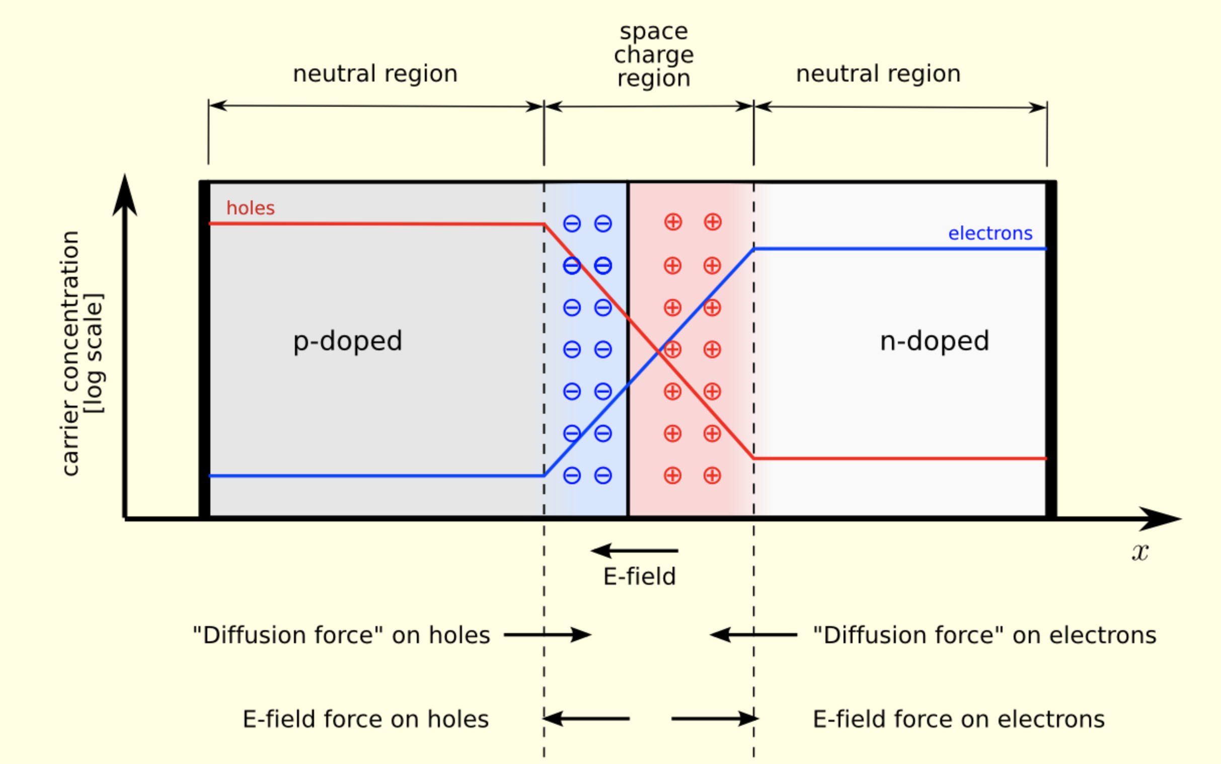
The diffusion current occurs because the majority carriers in each of the doped semiconductors will want to leave their current location in favor of a location with a lower density of their type of charge; this makes sense when you think about diffusion as being movement from high concentration to low concentration.

As a result of this movement, there will be an Electric field which is generated at the junction, that goes from N to P, because of the gradient in charge distribution (Note: The electric field is not constant in this area). What this causes is a drift current in the opposite direction of the diffusion current; this also makes sense when you think about drift as 'drifting in the direction of a river', since the charges move due to the E-fields.

enter image description here

The region where the E-field is present is what is referred to as the depletion region, the width of the depletion region is proportional to the potential difference of the Fermi-Energies which can be decreased with a forward bias, or increased with a reverse bias. This is why the PN junction can only conduct in one direction, and why there is a minimum voltage needed for the charges to overcome the energy barrier of the junction.

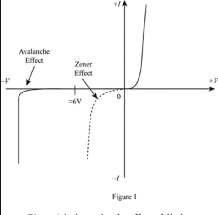
Note: There is also something caled Avalanche Breakdown/Zener Effect which is when the reverse bias is so large that the E-field cannot get large enough to fight the current and the P-N junction stops working as it ought to. See here: enter image description here

$\endgroup$

Your Answer

By clicking “Post Your Answer”, you agree to our terms of service and acknowledge you have read our privacy policy.

Not the answer you're looking for? Browse other questions tagged or ask your own question.