3
$\begingroup$

I have gotten myself confused about the band structure explanation of semi-conductors vs insulators. The Wikipedia picture

enter image description here

and the explanation surrounding it seem to suggest that Fermi Level is a property of the material. I understand how Fermi-Energy is a property of the material: it is the highest energy occupied by an electron at zero temperature. But Fermi level as shown in the picture doesn't make sense to me as there is nothing special about that level intrinsically for semi-conductors and insulators. Furthermore, there is no state there to occupy.

If I think of Fermi-Level as the external voltage (or chemical potential in the grand canonical ensemble) the pictures make sense but then its not an intrinsic property of the material (which is not the way its usually stated) and in that case I also do not see the difference between a semi-conductor and an insulator.

$\endgroup$

4 Answers 4

1
$\begingroup$

Let me first point out that Fermi level and Fermi energy are not the same thing (e.g., see here). What we are discussing here is mainly Fermi level (=chemical potential in the Fermi-Diract distribution), but the definition given in the OP is that of the Fermi energy: the highest energy occupied by an electron at zero temperature. They coincide in metals at zero temperature, but otherwise they are different (notably in the case of semiconductors, although these terms often get mixed).

It is an intrinsic property
If we take a pure material with a perfect crystal lattice at zero temperature, it will have Fermi level somewhere, and this position will be idnependent on the size and shape of the material. In this sense the Fermi level is an intrinsic property of a material. Depending on whether the Fermi level falls in the gap or not we can classify the materials in semiconductors/insulators. (This classification may get somewhat more complex, if we consider real materials with complex band shapes.)

Yet it can be modified
Chemical potential is however known to depend on temperature, so it can be changed. Moreover, we often deliberately change it by doping, i.e., by adding impurities. Similarly, imperfections of the crystal lattice will affect its position.

Another way to change Fermi level is by applying an electric field: e.g., in graphene or semiconductor nanostructures it is achieved by applying bias to the back gate, parallel to the material. It is also common to model bias applied to a nanostructure by a difference of Fermi levels on the two sides.

$\endgroup$
1
$\begingroup$

The material has defined density of the states of given energy $\rho(E)$. Then it can be proven that the number of the electrons of given energy follows the distbibution $$ n(E) = \rho(E) \frac{1}{1+e^{(E-E_F)/kT}} $$ with some (for now, unknown) parameter $E_F$. As the total number of electrons $N$ is also defined by the material, we have an equation $$ N = \int_0^\infty \rho(E) \frac{1}{1+e^{(E-E_F)/kT}} dE $$ which, in a convoluted way, defines what $E_F$ is. Therefore $E_F$ is defined by the properties of the material $(\rho(E)$, $N$), but also by the temperatue $T$. However, the depencence on the temperature is usually very weak and can be neglected. Because of that, from the practical point of view it's usually more useful to describe the material by the pair $(\rho(E), E_F)$ rather than $(\rho(E), N)$. We should remember however that $E_F$ isn't a fundamental property of the material, but a derived one.

Note that energy levels with $E<<E_F$ can't conduct because they are completely filled (and therefore these electrons can't easily change their state), and energy levels with $E>>E_F$ also can't conduct because they are completely empty and there's no electrons there that can change their state. Only the energy level of energy $E \approx E_F$ can conduct. The temperature $T$ defines the scale $kT$ which tells us how close to $E_F$ the electron actually needs to be to conduct.

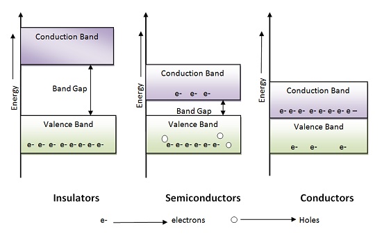
The fermi level defined in such a way can happen to have a value for which $\rho(E_F) > 0$, then we get a conductor, because close to the fermi level there will be plenty of partialy occupied energy levels that electrons can use to conduct electricity. If the Fermi Energy happens to be in a region where $\rho(E_F) = 0$ and there are no available nergy levels nearby, we get an insulator. If the Fermi Energy happens to be in a region where $\rho(E_F) = 0$ but there are some available energy levels nearby, we get a semiconductor, because these energy levels will be almost completely empty or almost completely filled, but not quite, so there will be a small amount of electrons or holes that can conduct electricity.

We can also see how additions to a semiconductor change the fermi level. They usually don't significantly change $\rho(E)$, but they can change $N$ enough so that the Fermi level $E_F$ changes significantly.

$E_F$ can also be affected if $\rho(E)$ is modified, for example by the external electric field, or in case of some materials, by mechanical stress, etc.

$\endgroup$
-1
$\begingroup$

Take a look at the Fermi-Dirac Distribution Function.

$f(E)=\frac{1}{e^{(\frac{E-E_F}{kT})}+1}$, and the Fermi Energy is the maximum energy such that $f(E)=0.5$, i.e. the probability of the quantum state being occupied by an electron is exactly half. By judging this equation, we can safely say that the Fermi energy is an intrinsic property of a material.

For an insulator, notice the large band gap. Take diamond, for instance. Diamond has a band gap of $5.5eV$, which is extremely large. However, for semiconductors, the band gap a relatively smaller, such as $1.1eV$ for silicon, which can be easily achieved when a potential difference is applied. In my opinion, the image there isn't a very good picture fo what happens. Check out the image below.

enter image description here

For the different types of semiconductors, such as p-type and n-type ones, the Fermi levels are lowered and raised due to the addition of trivalent or pentavalent elements respectively. For p-type semiconductors, the addition of trivalent elements result in more holes than electons, carrying a more positive charge. Hence, Fermi level drops down with less negative charge carriers. The opposite happens for n-type semiconductors. Hope this clears your doubt.

$\endgroup$
1
  • $\begingroup$ As far as I see, you did not really answer the question, rather you generlized the Fermi energy to non-zero temperature and then postulated that it is an intrinsic property. $\endgroup$ Commented Jul 7, 2018 at 12:47
-1
$\begingroup$

TL;DR: You can obtain the Fermi level from the band structure plus knowledge about the electron density of the crystal, both of which are intrinsic to the material.

Suppose the independent electron approximation (cf. Ashcroft & Mermin) holds valid for your crystal under consideration. Furthermore, assume that the crystal is finite with periodic boundary conditions (which does not affect the thermodynamic limit and hence can readily be assumed). Then the band structure of the crystal is an intrinsic property of the crystal. Indeed, it is just a clever way of visualizing the energy eigenvalues of electrons in the crystal and since we have a finite crystal there are only finitely many allowed crystal momenta. Hence, below any chosen energy value there are only finitely many energy eigenvalues of this system. Now assume there are $N$ electrons in our crystal. Note that the electron density is an intrinsic property of the crystal, hence the number of electrons $N$ is intrinsic as well as soon as we know the size of our crystal. If we now fill all of the $N$ lowest energy eigenstates of our crystal(/band structure) we end up with a highest occupied energy level, which we just call the Fermi Level. There is a slight variation of the definition in the case that above the highest occupied state there is a band gap, but still the Fermi level is completely instrinsic from our considerations.

What is now interesting is that since the number of allowed crystal momenta scales linearly with the spatial extent of the crystal, the number of eigenstates below any threshold scales proportional to the number of electrons in the crystal. Therefore, the Fermi level is even independent of the size of our sample and it is even more an intrinsic property.

In my considerations I assumed that I can think of filling up the energy level with "single independent electrons", which ignores a part of electron-electron interactions. Therefore, my argument will not extend to crystals in which the independent electron approximations breaks down.

$\endgroup$
1
  • $\begingroup$ This is in response to your comment '...we end up with a highest occupied energy level, which we just call the Fermi Level. " This works fine for conductors but how the Fermi Level end up being between two bands where there are no state? This is my original confusion. $\endgroup$ Commented Jul 9, 2018 at 9:46

Your Answer

By clicking “Post Your Answer”, you agree to our terms of service and acknowledge you have read our privacy policy.