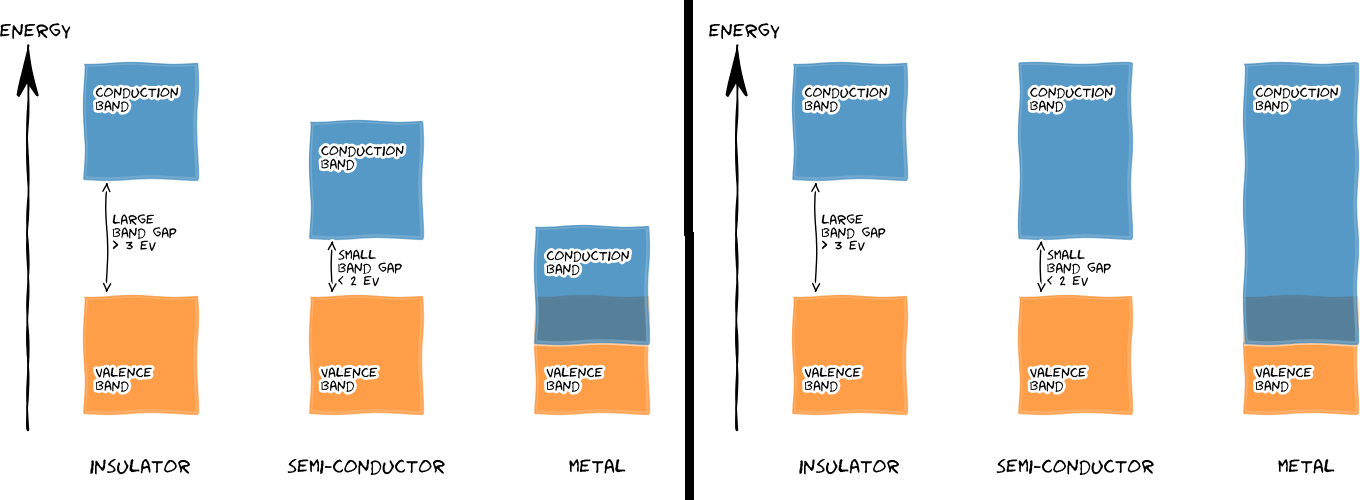
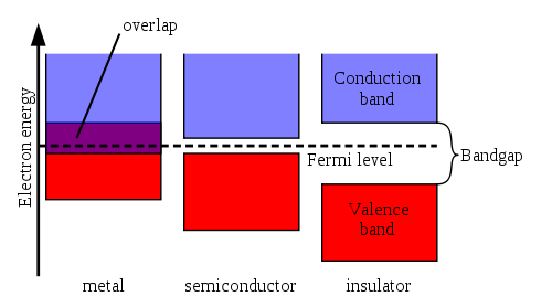
The energy band diagram is a model for describing why an insulator is not a good conductor compared to a semiconductor: in the first case, electrons would need to pass a very large band gap in order to promote from the valence band to the conduction band. The energy required for this is simply too large (and would lead to too much heat in the material).
For the semiconductor, on the other hand, the energy is smaller and electrons can move from the valence band to the conduction band by thermal excitation.
Fine, but which of the following figures is "more" correct, the one where the conduction is of the same thickness, or the one where the conduction bands' upper levels are the same?
The first one is more often used, but that might not mean too much. Any thoughts or ideas?


