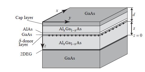
I have a question regarding the way in which one often constructs a two-dimensional electron gas in heterostructures. I have a specific example in mind, although I believe this is quite a common way to build the system if I can trust the literature. As shown in the diagram below (borrowed from Semiconductor Nanostructures by Thomas Ihn) we have a type 1 heterostructure with GaAs and AlGaAs. On top of that there is a $\delta$ doped donor layer (so there is one layer with heavy doping), above which there is another GaAs layer, an AlAs layer and another GaAs layer.
Now, I have a few questions about this. First of all I'm not entirely sure why we don't just make the 2DEG by sandwiching the GaAs layer between two AlGaAs layers (ABA) so that you have a quantum well in your conduction band, which then gives you your 2DEG, like in the diagram below. In my mind this is the most simple way of going about such a problem, but perhaps it is just too simplistic. You're not taking the surface into account and such.
But okay, let us continue. On top of the AlGaAs layer we have the $\delta$ donor layer. Why do we use this? I know that the idea of sheet doping is that you create an electrostatic potential and thus that (in the absence of other factors) you have donor electrons that are bound to the plane. But now in this system, because the layer is on top of the AlGaAs which has a larger band gap than GaAs, it is energetically favorable for the donor electrons to move towards the GaAs. On the other hand the positively charged donors also pull on these electrons. Is this then how we get our 2DEG? The donor electrons somehow get into a bound state at the interface?
I am not sure if this is the case, but perhaps it is. My final question would then be, if this is indeed so, why do we have all these additional layers on top? The GaAs, the AlAs, more AlGaAs, and more GaAs. I don't get the purpose of this. Perhaps it is related to surface states and Fermi level pinning or something?


