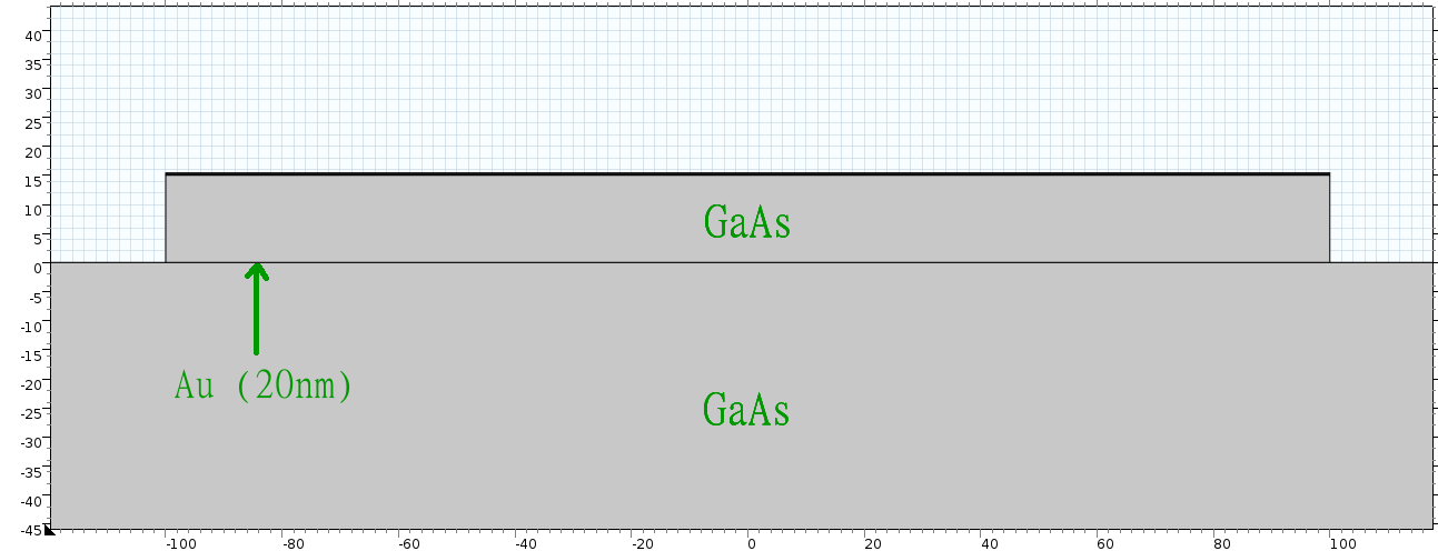
I am simulating a waveguide in COMSOL, a FEM solver. My model looks like this (it is similar to a standard Quantum Cascade Laser geometry):

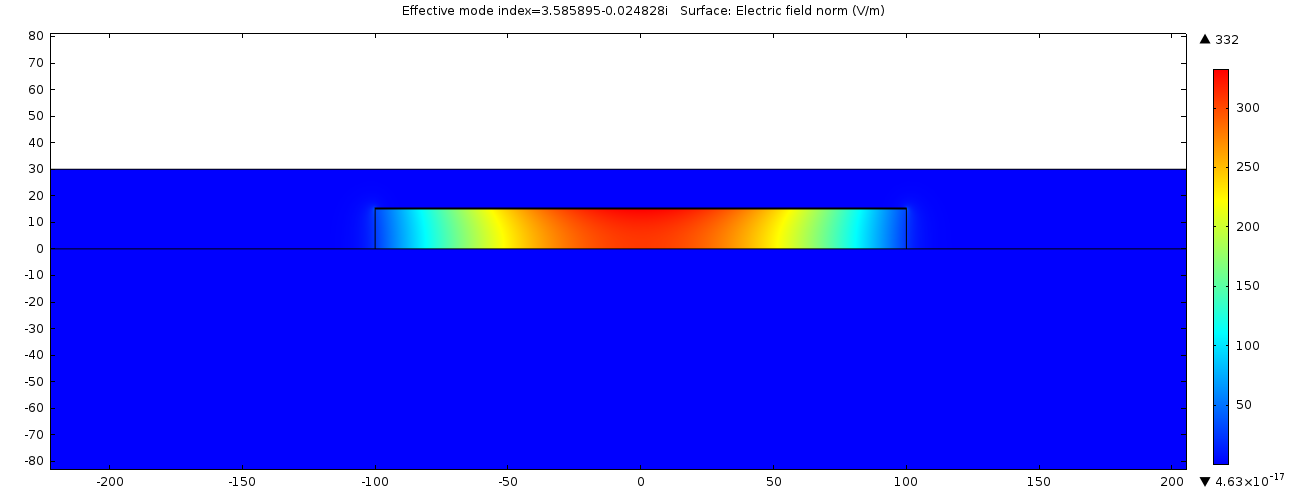
Therefore there is a very thin (30nm) layer of gold sandwiched by two regions consisting of Gallium Arsenide ($ \epsilon_r \simeq 13$). When I perform a mode analysis around 3THz (the frequency of my laser, $\simeq 100 \mu m$), the mode most likely to propagate (lowest losses, matching effective mode index) is the one below (E field norm is plotted here):

Now, I would expect this behaviour if the gold layer in between was thick enough, because the plasma frequency of the gold, according to the Drude model, is well above 3THz. The absorption coefficient is equal to
$$\alpha = \frac{2 \kappa \omega}{c}$$
and the skin depth, defined as $\delta = 2/ \alpha$, is around 40-50nm at this frequency. Therefore, due to the skin effect, the reflectivity of the thin gold layer would be very low and the wave would leak out into the bottom layer.
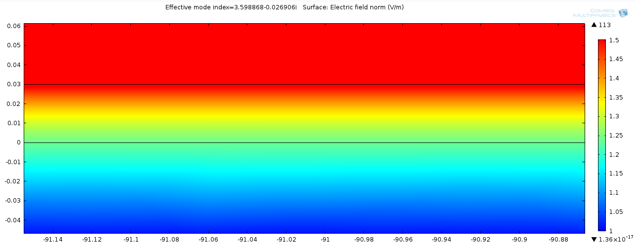
The E field does penetrate the gold, but decays very rapidly. This is the norm of E in the gold layer (0 to 0.03 on the y-axis), zoomed in a lot and the color range adjusted (notice $|E_{max}|>300$ on the original plot):

This is what I got from the support:
The reflection appears to be the result of the normal flux conservation boundary condition $Dy_1=Dy_2$. Since in the gold Er is much larger than in the material, $Ey_1<<Ey_2$. However, the tangential components of the electric field (which should indeed decay after one skin depth) are almost continuous thorough the gold thickness.
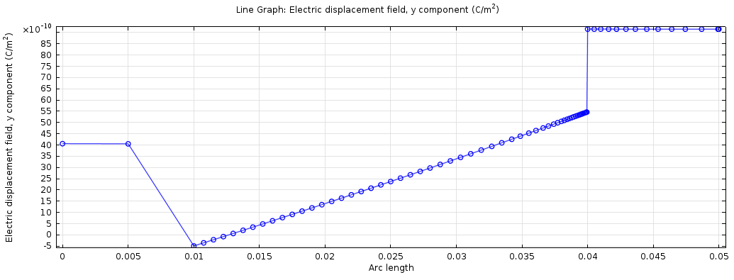
But when I look at the displacement current (y component), I get a clearly discontinuous plot:

I got another reply, commenting on this issue:
This discontinuity is attributed to transition between a conductor and a dielectric. The D1-D2=pho_s condition is derived from the charge conservation law, J1-J2=dt phos_s, where J1 and J2 are the sum of displacement and conduction currents. In case that the conductivity in both domains is zero, you get the electric flux conservation. When passing through a conductor-dielectric boundary, the induction current becomes discontinuous and therefor, the displacement current will too be discontinuous. The displacement current is directly related to the flux density. Thus you see the jump in the normal flux component. If you plot emw.Ex or emw.Jy you will see that they are continuous. The different current components (emw.Jiy, emw.Jdy) and emw.Dy will be discountinuous.
If I understand correctly, this just means that there will be charge accumulation on the Au/GaAs interface due to the existence of a Schottky junction.
Am I wrong in my assumptions, am I misunderstanding the skin effect, am I plotting the wrong thing? If not, why am I getting the wrong result? From the technical point of view, the mesh in the software is small enough to resolve the thin layer, so it can't be the problem.
