Commonmark migration
Source Link

Background

#Background# ConsiderConsider a normal metal (N) - superconductor (S) junction. Assume N is in the region $x<0$ and S is in the region $x>0$. In addition, let us assume that the system is invariant in the $y$ and $z$ directions such that the momentum parallel to the interface is conserved.

The system can be described by the BdG Hamiltonian of the form \begin{equation} \begin{bmatrix} H_e & \Delta\\ \Delta & -(H_e)^* \end{bmatrix} \begin{bmatrix} u(x,y,z)\\ v(x,y,z) \end{bmatrix} = E\begin{bmatrix} u(x,y,z)\\ v(x,y,z) \end{bmatrix}, \end{equation} where $\Delta = \Delta_0\theta(x)$, $H_e = -\frac{\hbar^2}{2m}\nabla^2 - \mu(x)$, and $\mu(x) = \mu>0$. Here $\Delta_0$, $m$, and $\mu$ are positive constants.

Question

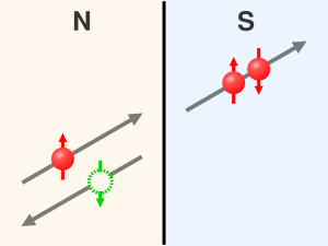
##Question## LetLet us assume that an electron is incident from N. By solving this equation for $x<0$ and $x>0$ we can obtain the reflection coefficient for normal reflection and Andreev reflection. I have read many places that the normal reflection is specular, while the Andreev reflection is retroreflective. By normal reflection I mean that the angle of incidence is equal to the angle of reflection. By retroreflection I mean the process sketched in the image below:

enter image description here

The filled red circle is an electron with spin up, the hollow dashed circle is a hole with spin down.

My question is why and how can one show from the BdG equation that the hole is always retroreflected? Alternatively Why is specular Andreev reflection forbidden in this simple case?

I'm asking this question because I would like to understand why one can have specular andreev reflection in graphene:

Andreev reflection and Klein tunneling in graphene

but not in the simple model above.

#Background# Consider a normal metal (N) - superconductor (S) junction. Assume N is in the region $x<0$ and S is in the region $x>0$. In addition, let us assume that the system is invariant in the $y$ and $z$ directions such that the momentum parallel to the interface is conserved.

The system can be described by the BdG Hamiltonian of the form \begin{equation} \begin{bmatrix} H_e & \Delta\\ \Delta & -(H_e)^* \end{bmatrix} \begin{bmatrix} u(x,y,z)\\ v(x,y,z) \end{bmatrix} = E\begin{bmatrix} u(x,y,z)\\ v(x,y,z) \end{bmatrix}, \end{equation} where $\Delta = \Delta_0\theta(x)$, $H_e = -\frac{\hbar^2}{2m}\nabla^2 - \mu(x)$, and $\mu(x) = \mu>0$. Here $\Delta_0$, $m$, and $\mu$ are positive constants.

##Question## Let us assume that an electron is incident from N. By solving this equation for $x<0$ and $x>0$ we can obtain the reflection coefficient for normal reflection and Andreev reflection. I have read many places that the normal reflection is specular, while the Andreev reflection is retroreflective. By normal reflection I mean that the angle of incidence is equal to the angle of reflection. By retroreflection I mean the process sketched in the image below:

enter image description here

The filled red circle is an electron with spin up, the hollow dashed circle is a hole with spin down.

My question is why and how can one show from the BdG equation that the hole is always retroreflected? Alternatively Why is specular Andreev reflection forbidden in this simple case?

I'm asking this question because I would like to understand why one can have specular andreev reflection in graphene:

Andreev reflection and Klein tunneling in graphene

but not in the simple model above.
Background

Consider a normal metal (N) - superconductor (S) junction. Assume N is in the region $x<0$ and S is in the region $x>0$. In addition, let us assume that the system is invariant in the $y$ and $z$ directions such that the momentum parallel to the interface is conserved.

The system can be described by the BdG Hamiltonian of the form \begin{equation} \begin{bmatrix} H_e & \Delta\\ \Delta & -(H_e)^* \end{bmatrix} \begin{bmatrix} u(x,y,z)\\ v(x,y,z) \end{bmatrix} = E\begin{bmatrix} u(x,y,z)\\ v(x,y,z) \end{bmatrix}, \end{equation} where $\Delta = \Delta_0\theta(x)$, $H_e = -\frac{\hbar^2}{2m}\nabla^2 - \mu(x)$, and $\mu(x) = \mu>0$. Here $\Delta_0$, $m$, and $\mu$ are positive constants.

Question

Let us assume that an electron is incident from N. By solving this equation for $x<0$ and $x>0$ we can obtain the reflection coefficient for normal reflection and Andreev reflection. I have read many places that the normal reflection is specular, while the Andreev reflection is retroreflective. By normal reflection I mean that the angle of incidence is equal to the angle of reflection. By retroreflection I mean the process sketched in the image below:

enter image description here

The filled red circle is an electron with spin up, the hollow dashed circle is a hole with spin down.

My question is why and how can one show from the BdG equation that the hole is always retroreflected? Alternatively Why is specular Andreev reflection forbidden in this simple case?

I'm asking this question because I would like to understand why one can have specular andreev reflection in graphene:

Andreev reflection and Klein tunneling in graphene

but not in the simple model above.

Source Link
MOOSE
  • 465
  • 5
  • 19

Why is Andreev reflection in a NS junction retroreflective?

#Background# Consider a normal metal (N) - superconductor (S) junction. Assume N is in the region $x<0$ and S is in the region $x>0$. In addition, let us assume that the system is invariant in the $y$ and $z$ directions such that the momentum parallel to the interface is conserved.

The system can be described by the BdG Hamiltonian of the form \begin{equation} \begin{bmatrix} H_e & \Delta\\ \Delta & -(H_e)^* \end{bmatrix} \begin{bmatrix} u(x,y,z)\\ v(x,y,z) \end{bmatrix} = E\begin{bmatrix} u(x,y,z)\\ v(x,y,z) \end{bmatrix}, \end{equation} where $\Delta = \Delta_0\theta(x)$, $H_e = -\frac{\hbar^2}{2m}\nabla^2 - \mu(x)$, and $\mu(x) = \mu>0$. Here $\Delta_0$, $m$, and $\mu$ are positive constants.

##Question## Let us assume that an electron is incident from N. By solving this equation for $x<0$ and $x>0$ we can obtain the reflection coefficient for normal reflection and Andreev reflection. I have read many places that the normal reflection is specular, while the Andreev reflection is retroreflective. By normal reflection I mean that the angle of incidence is equal to the angle of reflection. By retroreflection I mean the process sketched in the image below:

enter image description here

The filled red circle is an electron with spin up, the hollow dashed circle is a hole with spin down.

My question is why and how can one show from the BdG equation that the hole is always retroreflected? Alternatively Why is specular Andreev reflection forbidden in this simple case?

I'm asking this question because I would like to understand why one can have specular andreev reflection in graphene:

Andreev reflection and Klein tunneling in graphene

but not in the simple model above.