added 236 characters in body
Source Link

It's@user3533030 Makes a very good point, yet it may be an understatement.

"These problems are not easily solved analytically."


It's 5 years plus now since this question was asked. TheAnd not too much has improved. T junction should have been a thing of the past by now. Things are slowing improving.


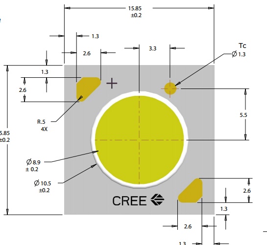
The manufactures now publish the temperature delta between T junction and T thermal pad, typically about 15°C. Some their recommend temperature values are relative to the LED's case temperature rather than T junction. For consistency, some manufacturers now include a Temperature "Spot" on the LED's case where you measure the temperature with a thermocouple.

The below image the Temperature Measurement spot is labeled Tc

enter image description here

The problem with the simulated modeling approach is LEDs have no "k" factor. They have no constant in any of their characteristics and the min/max delta is too great to produce modeled results with anything accurate enough to be meaningful. LEDs seem to be simple opto-electronic components, but they are not.

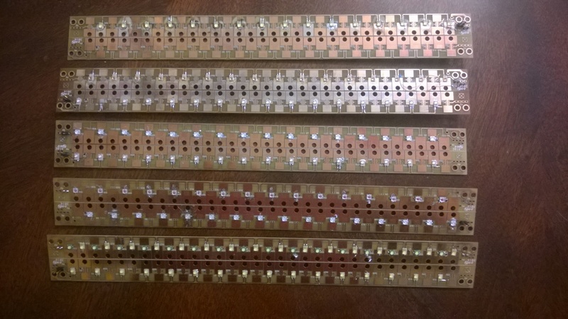
As I write this I am running an experiment with a new heatsink on a 12"x 0.7" PCB with 16 3 Watt LEDs (Cree XPE and Lumiled Rebel ES). The results of this modeling would be of little value.

enter image description here

You should concentrate your effort on the thermal management characteristics of the heatsink and PCB rather than the LED junction to thermal pad.

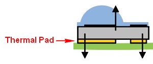
Another problem is the manufacturer's recommended circuit board designs. Still today, their recommendations consist of mostly how many holes, the diameter of the holes, and the distance between the holes to reduce the thermal resistance from the LED side of the board to the opposite side. That is because in their thermal model the PCB's thermal resistance is the greatest factor. A reduction in the PCB thermal resistance pays the greatest rewards. Except...

enter image description here

enter image description here

enter image description here

The problem with that approach is attaching the heatsink to the opposite side of the PCB. Why not increase the thickness of the copper on the LED side and attach the heatsink to the LED side of the board and take the PCB's thermal resistance out of the equation?

enter image description here

This has worked so well for me I have created a new problem. Condensation on the heatsink and PCB.

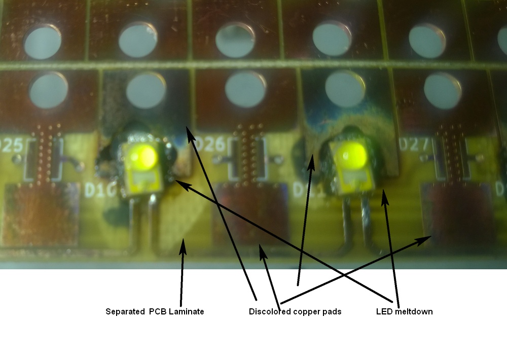
The PCB gets very hot without thermal management. After assembling the first test board I pumped 1 Amp through the LEDs. I do not know the temperature because the board got so hot so fast I didn't get a temperature reading before the board burned.

enter image description here

enter image description here

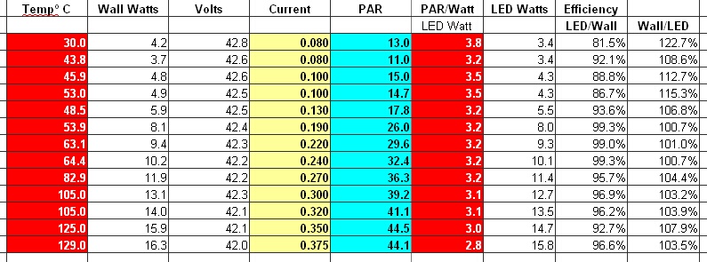
In a more sensible approach I was only able to measure up to 350mA before the temperature exceed the LED's maximum temperature.

  • PAR = photosynthetic active radiation

enter image description here

The results so far tonight are looking very well with a new heatsink, designed with off the shelf commodity parts, where the total parts cost is $3.50 per foot.

When compared with no thermal management @ 350mA = 125°C, I think I amymay be on to something without thermal junction modeling.
The point is as @ Stated by @user3533030 ,

Current=700mA
Thermal Pad °C
11:00 PM    28
11:05 PM    22
11:15 PM    23
11:25 PM    21.5
11:35 PM    21.3
11:55 PM    22.9
12:15 AM    22.4

It's 5 years plus now since this question was asked. The manufactures now publish the temperature delta between T junction and T thermal pad, typically about 15°C. Some their recommend temperature values are relative to the LED's case temperature rather than T junction. For consistency, some manufacturers now include a Temperature "Spot" on the LED's case where you measure the temperature with a thermocouple.

The below image the Temperature Measurement spot is labeled Tc

enter image description here

The problem with the simulated modeling approach is LEDs have no "k" factor. They have no constant in any of their characteristics and the min/max delta is too great to produce modeled results with anything accurate enough to be meaningful. LEDs seem to be simple opto-electronic components, but they are not.

As I write this I am running an experiment with a new heatsink on a 12"x 0.7" PCB with 16 3 Watt LEDs (Cree XPE and Lumiled Rebel ES). The results of this modeling would be of little value.

enter image description here

You should concentrate your effort on the thermal management characteristics of the heatsink and PCB rather than the LED junction to thermal pad.

Another problem is the manufacturer's recommended circuit board designs. Still today, their recommendations consist of mostly how many holes, the diameter of the holes, and the distance between the holes to reduce the thermal resistance from the LED side of the board to the opposite side. That is because in their thermal model the PCB's thermal resistance is the greatest factor. A reduction in the PCB thermal resistance pays the greatest rewards. Except...

enter image description here

enter image description here

enter image description here

The problem with that approach is attaching the heatsink to the opposite side of the PCB. Why not increase the thickness of the copper on the LED side and attach the heatsink to the LED side of the board and take the PCB's thermal resistance out of the equation?

enter image description here

This has worked so well for me I have created a new problem. Condensation on the heatsink and PCB.

The PCB gets very hot without thermal management. After assembling the first test board I pumped 1 Amp through the LEDs. I do not know the temperature because the board got so hot so fast I didn't get a temperature reading before the board burned.

enter image description here

enter image description here

In a more sensible approach I was only able to measure up to 350mA before the temperature exceed the LED's maximum temperature.

  • PAR = photosynthetic active radiation

enter image description here

The results so far tonight are looking very well with a new heatsink, designed with off the shelf commodity parts, where the total parts cost is $3.50 per foot.

When compared with no thermal management @ 350mA = 125°C, I think I amy be on to something without thermal junction modeling.
The point is as @ Stated by @user3533030 ,

Current=700mA
Thermal Pad °C
11:00 PM    28
11:05 PM    22
11:15 PM    23
11:25 PM    21.5
11:35 PM    21.3
11:55 PM    22.9
12:15 AM    22.4
@user3533030 Makes a very good point, yet it may be an understatement.

"These problems are not easily solved analytically."


It's 5 years plus now since this question was asked. And not too much has improved. T junction should have been a thing of the past by now. Things are slowing improving.


The manufactures now publish the temperature delta between T junction and T thermal pad, typically about 15°C. Some their recommend temperature values are relative to the LED's case temperature rather than T junction. For consistency, some manufacturers now include a Temperature "Spot" on the LED's case where you measure the temperature with a thermocouple.

The below image the Temperature Measurement spot is labeled Tc

enter image description here

The problem with the simulated modeling approach is LEDs have no "k" factor. They have no constant in any of their characteristics and the min/max delta is too great to produce modeled results with anything accurate enough to be meaningful. LEDs seem to be simple opto-electronic components, but they are not.

As I write this I am running an experiment with a new heatsink on a 12"x 0.7" PCB with 16 3 Watt LEDs (Cree XPE and Lumiled Rebel ES). The results of this modeling would be of little value.

enter image description here

You should concentrate your effort on the thermal management characteristics of the heatsink and PCB rather than the LED junction to thermal pad.

Another problem is the manufacturer's recommended circuit board designs. Still today, their recommendations consist of mostly how many holes, the diameter of the holes, and the distance between the holes to reduce the thermal resistance from the LED side of the board to the opposite side. That is because in their thermal model the PCB's thermal resistance is the greatest factor. A reduction in the PCB thermal resistance pays the greatest rewards. Except...

enter image description here

enter image description here

enter image description here

The problem with that approach is attaching the heatsink to the opposite side of the PCB. Why not increase the thickness of the copper on the LED side and attach the heatsink to the LED side of the board and take the PCB's thermal resistance out of the equation?

enter image description here

This has worked so well for me I have created a new problem. Condensation on the heatsink and PCB.

The PCB gets very hot without thermal management. After assembling the first test board I pumped 1 Amp through the LEDs. I do not know the temperature because the board got so hot so fast I didn't get a temperature reading before the board burned.

enter image description here

enter image description here

In a more sensible approach I was only able to measure up to 350mA before the temperature exceed the LED's maximum temperature.

  • PAR = photosynthetic active radiation

enter image description here

The results so far tonight are looking very well with a new heatsink, designed with off the shelf commodity parts, where the total parts cost is $3.50 per foot.

When compared with no thermal management @ 350mA = 125°C, I think I may be on to something without thermal junction modeling.

Current=700mA
Thermal Pad °C
11:00 PM    28
11:05 PM    22
11:15 PM    23
11:25 PM    21.5
11:35 PM    21.3
11:55 PM    22.9
12:15 AM    22.4
added 19 characters in body
Source Link

It's 5 years plus now since this question was asked. The manufactures now publish the temperature delta between T junction and T thermal pad, typically about 15°C. Some their recommend temperature values are relative to the LED's case temperature rather than T junction. For consistency, some manufacturers now include a Temperature "Spot" on the LED's case where you measure the temperature with a thermocouple.

The below image the Temperature Measurement spot is labeled Tc

enter image description here

The problem with the simulated modeling approach is LEDs have no "k" factor. They have no constant in any of their characteristics and the min/max delta is too great to produce modeled results with anything accurate enough to be meaningful. LEDs seem to be simple opto-electronic components, but they are not.

As I write this I am running an experiment with a new heatsink on a 12"x 0.7" PCB with 16 3 Watt LEDs (Cree XPE and Lumiled Rebel ES). The results of this modeling would be of little value.

enter image description here

You should concentrate your effort on the thermal management characteristics of the heatsink and PCB rather than the LED junction to thermal pad.

Another problem is the manufacturer's recommended circuit board designs. Still today, their recommendations consist of mostly how many holes, the diameter of the holes, and the distance between the holes to reduce the thermal resistance from the LED side of the board to the opposite side. That is because in their thermal model the PCB's thermal resistance is the greatest factor. A reduction in the PCB thermal resistance pays the greatest rewards. Except...

enter image description here

enter image description here

enter image description here

The problem with that approach is attaching the heatsink to the opposite side of the PCB. Why not increase the thickness of the copper on the LED side and attach the heatsink to the LED side of the board and take the PCB's thermal resistance out of the equation?

enter image description here

This has worked so well for me I have created a new problem. Condensation on the heatsink and PCB.

The PCB gets very hot without thermal management. After assembling the first test board I pumped 1 Amp through the LEDs. I do not know the temperature becasuebecause the board got so hot so fast I didn't get a temperature reading soon enough. Thebefore the board burned.

enter image description here   

enter image description here

In a more sensible approach I was only able to measure up to 350mA before the temperature exceed the LED's maximum temperature.

  • PAR = photosynthetic active radiation

enter image description here

The results so far tonight are looking very well with a new heatsink, designed with off the shelf commodity parts, where the total parts cost is $3.50 per foot.

When compared with no thermal management @ 350mA = 125°C, I think I amy be on to something without thermal junction modeling.
The point is as @ Stated by @user3533030 ,

Current=700mA
Thermal Pad °C
11:00 PM    28
11:05 PM    22
11:15 PM    23
11:25 PM    21.5
11:35 PM    21.3
11:55 PM    22.9
12:15 AM    22.4
It's 5 years plus now since this question was asked. The manufactures now publish the temperature delta between T junction and T thermal pad, typically about 15°C. Some their recommend temperature values are relative to the LED's case temperature rather than T junction. For consistency, some manufacturers now include a Temperature "Spot" on the LED's case where you measure the temperature with a thermocouple.

The below image the Temperature Measurement spot is labeled Tc

enter image description here

The problem with the simulated modeling approach is LEDs have no "k" factor. They have no constant in any of their characteristics and the min/max delta is too great to produce modeled results with anything accurate enough to be meaningful. LEDs seem to be simple opto-electronic components, but they are not.

As I write this I am running an experiment with a new heatsink on a 12"x 0.7" PCB with 16 3 Watt LEDs (Cree XPE and Lumiled Rebel ES). The results of this modeling would be of little value.

enter image description here

You should concentrate your effort on the thermal management characteristics of the heatsink and PCB rather than the LED junction to thermal pad.

Another problem is the manufacturer's recommended circuit board designs. Still today, their recommendations consist of mostly how many holes, the diameter of the holes, and the distance between the holes to reduce the thermal resistance from the LED side of the board to the opposite side. That is because in their thermal model the PCB's thermal resistance is the greatest factor. A reduction in the PCB thermal resistance pays the greatest rewards. Except...

enter image description here

enter image description here

enter image description here

The problem with that approach is attaching the heatsink to the opposite side of the PCB. Why not increase the thickness of the copper on the LED side and attach the heatsink to the LED side of the board and take the PCB's thermal resistance out of the equation?

enter image description here

This has worked so well for me I have created a new problem. Condensation on the heatsink and PCB.

The PCB gets very hot without thermal management. After assembling the first test board I pumped 1 Amp through the LEDs. I do not know the temperature becasue the board got so hot so fast I didn't get a reading soon enough. The board burned.

enter image description here  enter image description here

In a more sensible approach I was only able to measure up to 350mA before the temperature exceed the maximum temperature.

  • PAR = photosynthetic active radiation

enter image description here

The results so far tonight are looking very well with a new heatsink, designed with off the shelf commodity parts, where the total parts cost is $3.50 per foot.

Current=700mA
Thermal Pad °C
11:00 PM    28
11:05 PM    22
11:15 PM    23
11:25 PM    21.5
11:35 PM    21.3
11:55 PM    22.9
12:15 AM    22.4

It's 5 years plus now since this question was asked. The manufactures now publish the temperature delta between T junction and T thermal pad, typically about 15°C. Some their recommend temperature values are relative to the LED's case temperature rather than T junction. For consistency, some manufacturers now include a Temperature "Spot" on the LED's case where you measure the temperature with a thermocouple.

The below image the Temperature Measurement spot is labeled Tc

enter image description here

The problem with the simulated modeling approach is LEDs have no "k" factor. They have no constant in any of their characteristics and the min/max delta is too great to produce modeled results with anything accurate enough to be meaningful. LEDs seem to be simple opto-electronic components, but they are not.

As I write this I am running an experiment with a new heatsink on a 12"x 0.7" PCB with 16 3 Watt LEDs (Cree XPE and Lumiled Rebel ES). The results of this modeling would be of little value.

enter image description here

You should concentrate your effort on the thermal management characteristics of the heatsink and PCB rather than the LED junction to thermal pad.

Another problem is the manufacturer's recommended circuit board designs. Still today, their recommendations consist of mostly how many holes, the diameter of the holes, and the distance between the holes to reduce the thermal resistance from the LED side of the board to the opposite side. That is because in their thermal model the PCB's thermal resistance is the greatest factor. A reduction in the PCB thermal resistance pays the greatest rewards. Except...

enter image description here

enter image description here

enter image description here

The problem with that approach is attaching the heatsink to the opposite side of the PCB. Why not increase the thickness of the copper on the LED side and attach the heatsink to the LED side of the board and take the PCB's thermal resistance out of the equation?

enter image description here

This has worked so well for me I have created a new problem. Condensation on the heatsink and PCB.

The PCB gets very hot without thermal management. After assembling the first test board I pumped 1 Amp through the LEDs. I do not know the temperature because the board got so hot so fast I didn't get a temperature reading before the board burned.

enter image description here 

enter image description here

In a more sensible approach I was only able to measure up to 350mA before the temperature exceed the LED's maximum temperature.

  • PAR = photosynthetic active radiation

enter image description here

The results so far tonight are looking very well with a new heatsink, designed with off the shelf commodity parts, where the total parts cost is $3.50 per foot.

When compared with no thermal management @ 350mA = 125°C, I think I amy be on to something without thermal junction modeling.
The point is as @ Stated by @user3533030 ,

Current=700mA
Thermal Pad °C
11:00 PM    28
11:05 PM    22
11:15 PM    23
11:25 PM    21.5
11:35 PM    21.3
11:55 PM    22.9
12:15 AM    22.4
added 19 characters in body
Source Link

It's 5 years plus now since this question was asked. The manufactures now publish the temperature delta between T junction and T thermal pad, typically about 15°C. Some their recommend temperature values are relative to the LED's case temperature rather than T junction. For consistency, some manufacturers now include a Temperature "Spot" on the LED's case where you measure the temperature with a thermocouple.

The below image the Temperature Measurement spot is labeled Tc

enter image description here

The problem with the simulated modeling approach is LEDs have no "k" factor. They have no constant in any of their characteristics and the min/max delta is too great to produce modeled results with anything accurate enough to be meaningful. LEDs seem to be simple opto-electronic components, but they are not.

As I write this I am running an experiment with a new heatsink on a 12"x 0.7" PCB with 16 3 Watt LEDs (Cree XPE and Lumiled Rebel ES). The results of this modeling would be of little value.

enter image description here

You should concentrate your effort on the thermal management characteristics of the heatsink and PCB rather than the LED junction to thermal pad.

Another problem is the manufacturer's recommended circuit board designs. Still today, their recommendationrecommendations consist of mostly how many holes, the diameter of the holes, and the distance between the holes to reduce the thermal resistance from the LED side of the board to the opposite side. That is because in their thermal model the PCB's thermal resistance is the greatest factor. A reduction in the PCB thermal resistance pays the greatest rewards. Except...

enter image description here

enter image description here

enter image description here

The problem with that approach is attaching the heatsink to the opposite side of the PCB. Why not increase the thickness of the copper on the LED side and attach the heatsink to the LED side of the board and take the PCB's thermal resistance out of the equation?

enter image description here

This has worked so well for me I have created a new problem. Condensation on the heatsink and PCB.

The PCB gets very hot without thermal management. After assembling the first test board I pumped 1 Amp through the LEDs. I do not know the temperature becasue the board got so hot so fast I didn't get a reading soon enough. The board burned.

enter image description here enter image description here

In a more sensible approach I was only able to measure up to 350mA before the temperature exceed the maximum temperature.

  • PAR = photosynthetic active radiation

enter image description here

The results so far tonight are looking very well with a new heatsink, designed with off the shelf commodity parts, where the total parts cost is $3.50 per foot.

Current=700mA
Thermal Pad °C
11:00 PM    28
11:05 PM    22
11:15 PM    23
11:25 PM    21.5
11:35 PM    21.3
11:55 PM    22.9
12:15 AM    22.4

It's 5 years plus now since this question was asked. The manufactures now publish the temperature delta between T junction and T thermal pad, typically about 15°C. Some their recommend temperature values are relative to the LED's case temperature rather than T junction. For consistency, some manufacturers now include a Temperature "Spot" on the LED's case where you measure the temperature with a thermocouple.

The below image the Temperature Measurement spot is labeled Tc

enter image description here

The problem with the simulated modeling approach is LEDs have no "k" factor. They have no constant in any of their characteristics and the min/max delta is too great to produce modeled results with anything accurate enough to be meaningful. LEDs seem to be simple opto-electronic components, but they are not.

As I write this I am running an experiment with a new heatsink on a 12"x 0.7" PCB with 16 3 Watt LEDs (Cree XPE and Lumiled Rebel ES). The results of this modeling would be of little value.

enter image description here

You should concentrate your effort on the thermal management characteristics of the heatsink and PCB rather than the LED junction to thermal pad.

Another problem is the manufacturer's recommended circuit board designs. Still their recommendation consist of mostly how many holes, the diameter of the holes, and the distance between the holes to reduce the thermal resistance from the LED side of the board to the opposite side. That is because in their thermal model the PCB's thermal resistance is the greatest factor. A reduction in the PCB thermal resistance pays the greatest rewards.

enter image description here

enter image description here

enter image description here

The problem with that approach is attaching the heatsink to the opposite side of the PCB. Why not increase the thickness of the copper on the LED side and attach the heatsink to the LED side of the board and take the PCB's thermal resistance out of the equation?

enter image description here

This has worked so well for me I have created a new problem. Condensation on the heatsink and PCB.

The PCB gets very hot without thermal management. After assembling the first test board I pumped 1 Amp through the LEDs. I do not know the temperature becasue the board got so hot so fast I didn't get a reading soon enough. The board burned.

enter image description here enter image description here

In a more sensible approach I was only able to measure up to 350mA before the temperature exceed the maximum temperature.

  • PAR = photosynthetic active radiation

enter image description here

The results so far tonight are looking very well with a new heatsink, designed with off the shelf commodity parts, where the total parts cost is $3.50 per foot.

Current=700mA
Thermal Pad °C
11:00 PM    28
11:05 PM    22
11:15 PM    23
11:25 PM    21.5
11:35 PM    21.3
11:55 PM    22.9
12:15 AM    22.4
It's 5 years plus now since this question was asked. The manufactures now publish the temperature delta between T junction and T thermal pad, typically about 15°C. Some their recommend temperature values are relative to the LED's case temperature rather than T junction. For consistency, some manufacturers now include a Temperature "Spot" on the LED's case where you measure the temperature with a thermocouple.

The below image the Temperature Measurement spot is labeled Tc

enter image description here

The problem with the simulated modeling approach is LEDs have no "k" factor. They have no constant in any of their characteristics and the min/max delta is too great to produce modeled results with anything accurate enough to be meaningful. LEDs seem to be simple opto-electronic components, but they are not.

As I write this I am running an experiment with a new heatsink on a 12"x 0.7" PCB with 16 3 Watt LEDs (Cree XPE and Lumiled Rebel ES). The results of this modeling would be of little value.

enter image description here

You should concentrate your effort on the thermal management characteristics of the heatsink and PCB rather than the LED junction to thermal pad.

Another problem is the manufacturer's recommended circuit board designs. Still today, their recommendations consist of mostly how many holes, the diameter of the holes, and the distance between the holes to reduce the thermal resistance from the LED side of the board to the opposite side. That is because in their thermal model the PCB's thermal resistance is the greatest factor. A reduction in the PCB thermal resistance pays the greatest rewards. Except...

enter image description here

enter image description here

enter image description here

The problem with that approach is attaching the heatsink to the opposite side of the PCB. Why not increase the thickness of the copper on the LED side and attach the heatsink to the LED side of the board and take the PCB's thermal resistance out of the equation?

enter image description here

This has worked so well for me I have created a new problem. Condensation on the heatsink and PCB.

The PCB gets very hot without thermal management. After assembling the first test board I pumped 1 Amp through the LEDs. I do not know the temperature becasue the board got so hot so fast I didn't get a reading soon enough. The board burned.

enter image description here enter image description here

In a more sensible approach I was only able to measure up to 350mA before the temperature exceed the maximum temperature.

  • PAR = photosynthetic active radiation

enter image description here

The results so far tonight are looking very well with a new heatsink, designed with off the shelf commodity parts, where the total parts cost is $3.50 per foot.

Current=700mA
Thermal Pad °C
11:00 PM    28
11:05 PM    22
11:15 PM    23
11:25 PM    21.5
11:35 PM    21.3
11:55 PM    22.9
12:15 AM    22.4
added 129 characters in body
Source Link
Loading
added 80 characters in body
Source Link
Loading
Source Link
Loading